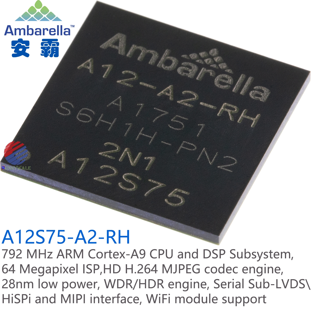
A12S75 Ambarella 792 MHz ARM Cortex-A9 CPU and DSP Subsystem, 64 Megapixel ISP,HD H.264 MJPEG codec engine, 28nm low power, WDR/HDR engine, Serial Sub-LVDS\ HiSPi and MIPI interface, WiFi support
2024-09-07 20:08:33
Buy Now
A12S75-A2-RH datasheet, System on Chip (SoC) platform for Ambarella action cameras,Ambarella ARM cortex-A9 CPU, Digital Signal Processing (DSP) subsystem,64MP image sensor pipeline ISP,H.264/MJPEG encoder engine,28NM low power,WDR/HDR, support Serial Sub-LVDS\
HiSPi and MIPI interface,WiFi support, Ambarella sports camera chip, support 64 million pixel controller,1080P@100 frame, A12S75 instruction manual
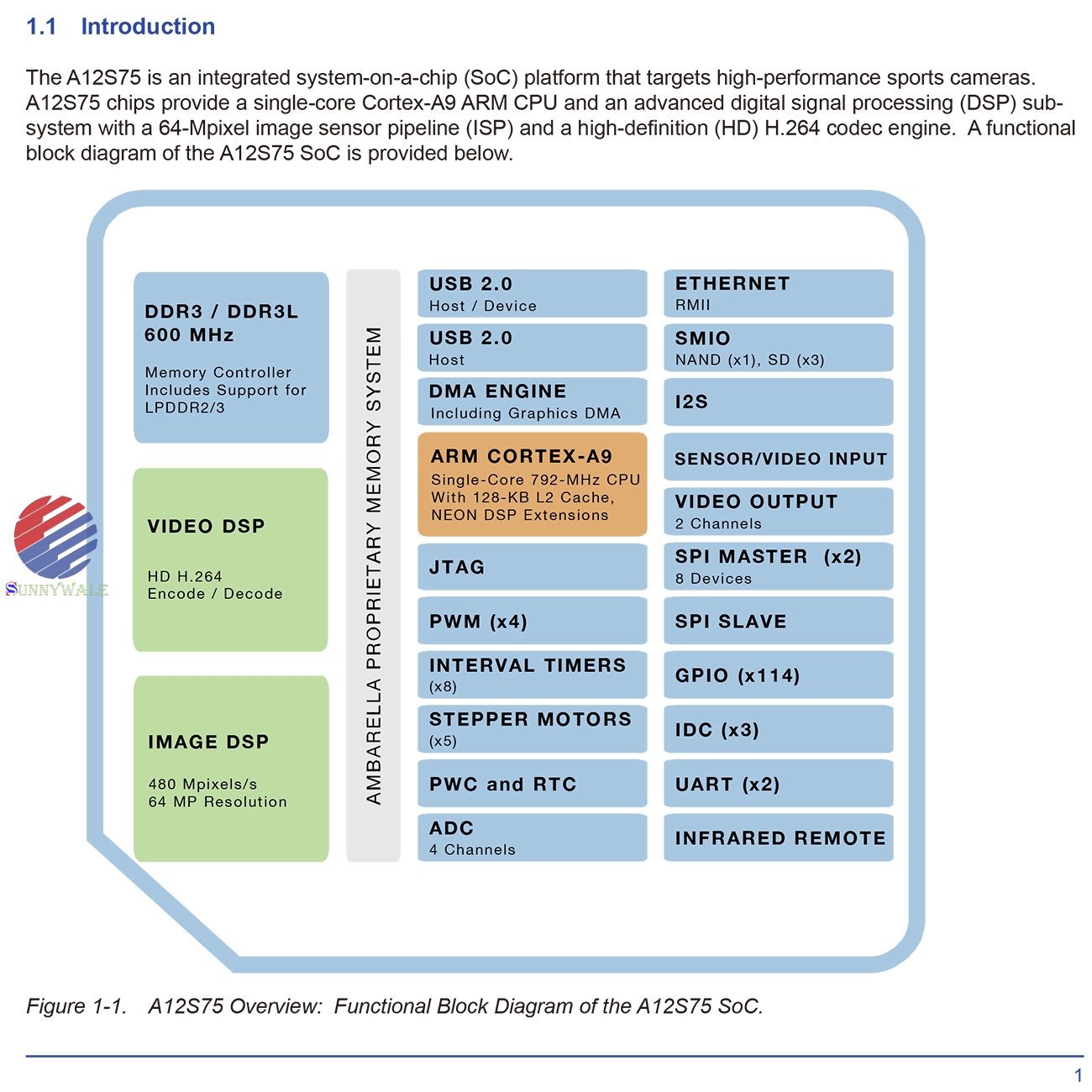
The A12S75 is an integrated system-on-a-chip (SoC) platform that targets high-performance sports cameras.
A12S75 chips provide a 792 MHz ARM Cortex-A9 CPU and an advanced Digital Signal Processing (DSP) subsystem with a 64-Mpixel Image Sensor Pipeline (ISP) and a high-definition (HD) H.264 codec engine.
● Embedded ARM cortex-A9 792 NHz CPU
● More than 480 MPixel/s processing rate
⊙ 64-MPixel maximum resolution
● Fish-eye lens dewarping and barrel distortion correction
● Advanced motion-compensated sharpening
● Advanced dynamic range (WDR and HDR) engine
● H.264 BP/MP/HP Level 5.1 and MJPEG co-decs
● Encode performance up to 1080P@100fps
● 114 General Purpose Input/Output (GPIO) short-height pins
● 404-pin TFBGA package (15 mm x 15 mm)
● 28-nm CMOS Low Power (LP) technology
1. A12S75 OVERVIEW
This preliminary datasheet for the A12S75 processor from Ambarella begins with a brief introduction to the chip
(Section 1.1) and a summary of key features (Section 1.2). chapter 2 describes the A12S75 peripheral interfac-
es. For pin details and electrical characteristics refer to chapter 3 and chapter 4, respectively. See chapter 5 for
package information and chapter 6 for Ambarella contact and ordering details.
Please note that the chip features described in this datasheet are subject to change. Details that have not been
entirely finalized (e.g., encoding specifics) are provided using conservative estimates (i.e., final encoding perfor-
mance is expected to meet or exceed the estimate provided). Please contact an Ambarella representative for
additional information.
1.1 A12S75 Introduction
The A12S75 is an integrated system-on-a-chip (SoC) platform that targets high-performance sports cameras.
A12S75 chips provide a single-core cortex-A9 ARM CPU and an advanced digital signal processing (DSP) sub-
system with a 64-Mpixel image sensor pipeline (ISP) and a high-definition (HD) H.264 codec engine. A functional
block diagram of the A12S75 Soc is provided below.
(Figure 1-1. A12S75 Overview: Functional Block Diagram of the A12S75 SoC.)
The A12S75 Soc provides a glueless interface to Serial Sub-LVDS, HiSPi, and mIPI interfaces, as well as parallel
connections to popular CMOS image sensors. The ISP offers advanced image-processing features, including
improved high dynamic range (HDR) processing with multi-exposure fusion, wide dynamic range (WDR) local
contrast enhancement, 3D motion-compensated noise reduction (MCTF), edge enhancement, 3A, image stabili-
zation, and dewarping.
The H.264 codec engine delivers versatile encoding up to 1920x1080p100 total performance. The high-efficiency
H.264 encoder implements progressive refresh for low-latency operations, as well as advanced main and High-
Profile functions for the highest-quality and lowest possible bitrate. These functions include bidirectional predic-
tion (B-frames), large motion-estimation search range, and macroblock-level quantization. Ambarella builds in
flexibility with a multi-streaming function, allowing on-the-fly start/stop as well as the adjustment of the bitrate,
frame rate, and GOP of each individual stream. The A12S75 WiFi module supports fast-action capture with loop
recording, remote view finders, and remote control by handheld devices.
A 792 MHz ARM Cortex-A9 CPU with NEON DSP extensions and floating point support is available for imple-
menting full-featured user applications.
The A12 family is fabricated using low-power 28-nm CMOS technology and integrates advanced power-saving
modes, such as utilizing DSP-subsystem memory resources to reduce external memory bandwidth and total cam-
era system power requirements.
1.2 A12S75 Feature List
Features of the A12S75 chip include:
● Embedded single-core ARM cortex-A9 CPU
⊙ Clock frequency up to 792 MHz
⊙ 32-Kbyte data / 32-Kbyte instruction cache
⊙ 128-Kbyte L2 cache
⊙ NEON SIMD engine
● DDR3 and DDR3L controller
⊙ Up to 600-MHz clock rate
⊙ 32-bit wide data bus
⊙ maximum capacity of 8 Gbits (1 Gbyte)
⊙ Includes support for the LPDDR2 and LPDDR3 low-power DDR interfaces
● Image pipeline
⊙ More than 480 mPixel/s processing rate
⊙ 64-mPixel maximum resolution
⊙ Fish-eye lens dewarping and barrel distortion correction
⊙ Black level correction
⊙ Dynamic and static defect pixel cluster correction
⊙ CFA crosstalk and fixed-pattern noise reduction
⊙ RGb bayer demosaicing
⊙ Lens shading
⊙ 3D LUT color transform with gamma
⊙ Advanced motion-compensated sharpening
⊙ Advanced dynamic range (WDR and HDR) engine with multi-exposure fusion and motion artifact reduction
⊙ Per-pixel local exposure dynamic range enhancement
⊙ Tone mapping and global tone-curve adjustment
⊙ Chromatic aberration correction
⊙ Flexible APIs and image-tuning tools
⊙ Adjustable 3A; exposure, white balance and focus control (AE/AWB/AF)
⊙ Day/Night and DC/P iris control
⊙ Crop, mirror, flip, 90°/270° rotation
⊙ Image stabilization with rolling shutter compensation
● Video engine
⊙ H.264 BP/mP/HP Level 5.1 and MJPEG codecs
⊙ Maximum encode performance:
- 1920x1080P@100fps
- 1280x720P@240fps
⊙ Advanced H.264 compression tools
- I, IP, IBP modes (M=1,2,3,4…; IP, IBP, IBBP, IBBBP…)
- High Profile with B-frames and hierarchical GOP
- Up to three reference frames
⊙ Flexible rate control
- CBR, VBR and constant QP with max bitrate control
- Macroblock-level adaptive quantization
⊙ 3D noise reduction (MCTF)
● Sensor/Video Input (VIN) interface
⊙ multiple input modes
- Supports up to 8-lane SLVS / HiSPi input and up to 4-lane mIPI input
- Support for 14-bit parallel and LVCMOS sensors
⊙ Support for popular CMOS sensors; Aptina, Sony, OV, Panasonic, Samsung
⊙ Two clocking options (PLL-generated GCLK_VIN or SLVS bit clock)
⊙ 16-bit CCIR.601 video input with external sync signals
⊙ 8-bit, 10-bit, 12-bit or 14-bit bT.656 video input with embedded sync codes including full-data-range support
● Video Output (VOUT) interfaces
⊙ Two logical channels to drive three video output ports
- One logical channel drives HDMI or analog
- One logical channel drives digital
⊙ Popular LCD panel controllers (RGb mode)
⊙ Support for RGBA and YUVA OSD
⊙ Video DAC for 480i/576i composite PAL/NTSC output
⊙ BT.656 embedded sync YUV output (8-bit or 16-bit mode)
⊙ HDMI 1.4b output with consumer Electronics control (CEC) and on-chip PHY
● AHb bus DMA controller
⊙ Memory-to-memory transfers including support for transfers between memory and peripherals
⊙ Programmable transfer count up to 4 mb
⊙ DMA scatter/gather via chained descriptor list in memory with DMA control information source
● Dedicated DMA co-processor for graphics and image operations
⊙ Offers linear copy, 2-D copy, composite, and alpha-blend image operations
⊙ Supports 4- to 32-bit pixel formats
● I2S digital audio interface (stereo)
⊙ Audio encoding/decoding
● Ethernet mAc controller
⊙ IEEE 802.3 compliant with full- and half-duplex (IEEE 802.3x flow-control) and Jumbo frames
⊙ IEEE 802.1Q VLAN tag detection
⊙ checksum off-load for received IP and TCP/UDP packets
⊙ Dedicated pins for RmII or mII interface
⊙ FIFO (2 Kb / 2 Kb) and DMA support
● Two USb 2.0 interfaces
⊙ One host and one configurable host/device interface, each with built-in PHY
● Flexible Storage media Input / Output (SMIO) interface
⊙ NAND Flash controller
- Up to 8-Gbit device, 512-byte and 2-Kbyte page sizes
- 8-bit flash chip data bus
- 4-bit and 8-bit SLC with ECC hardware and read-confirm support
- bcH error correction and increased spare area available
⊙ Three SD controllers (SD0, SD1, SD2)
- SD0:
● SDIO v3.0, SD, SDHc, SDXc, mmc and emmc operation with boot support and UHS-I speed
- SD1:
◎ SDIO v3.0, SD, SDHc, SDXc, mmc and emmc operation
- SD2:
◎ SDIO v1.0, SD, SDHc, SDXc, mmc and emmc operation
- 32-Gbyte maximum capacity for SDHc SD card
- 2-Tbyte maximum capacity for SDXC SD card
- 1-bit, 4-bit and 8-bit SD modes, cRc7 for command and cRc16 for data integrity
● Multiple boot options
⊙ NOR-SPI, NAND Flash, USb and emmc
● Vector interrupt controller including VIC CPU-offload functionality
● SSI / SPI controller interfaces
⊙ Two SSI / SPI masters with up to eight device enables
⊙ One dedicated SSI / SPI slave port to connect to an external system master
● Two-wire serial Inter-Integrated circuit (IDC) interfaces (x3)
⊙ Configurable IDC buses (x2)
⊙ One IDC bus dedicated for use with HDMI
● UART interface (x2)
⊙ DMA support
⊙ One interface supports flow control
● Infrared remote receiver interface which supports most popular protocols
● 114 General Purpose Input/Output (GPIO) short-height pins with individual pull-up/down control
● ADC (four channels) with high/low threshold interrupt generation and 12-bit resolution
● Built-in power controller for power-up/down sequencing
● Real Time clock (RTC)
● Interval timing with eight general-purpose timers configurable as external event counters
● Watchdog timer (one)
● Stepper motor interface (five channels) with four-channel Micro-Stepper interface
● Four Pulse Width modulators (PWM)
● JTAG In-circuit Emulator (ICE) interface for debugging (one)
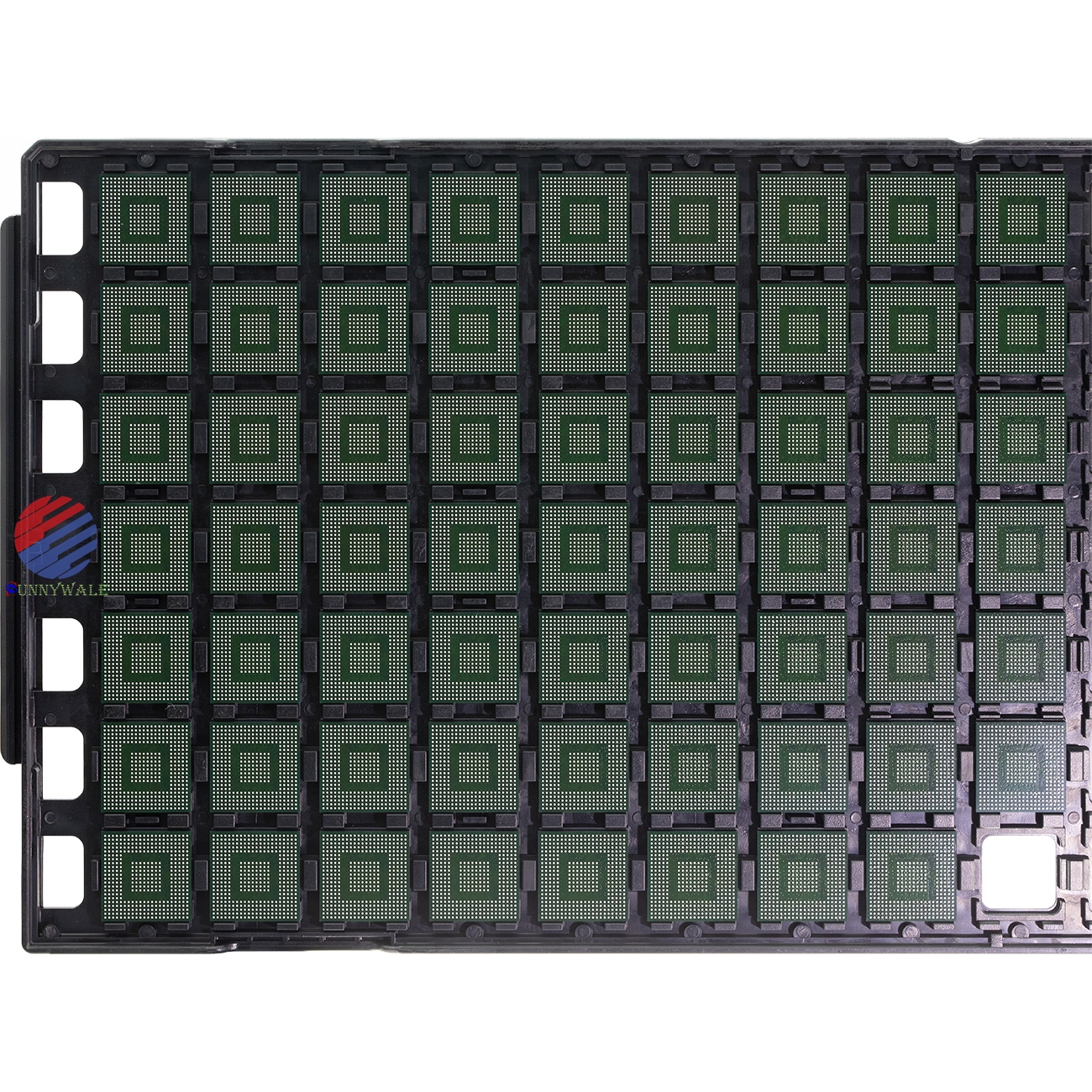
● 404-pin TFBGA package (15 mm x 15 mm)
● 28-nm CMOS Low Power (LP) technology
● Operating temperature from 0 ℃ to 70 ℃
2. A12S75 INTERFACES
2.1 Overview
This section summarizes the peripheral interfaces for the A12S75 chip as follows:
● (Section 2.2) SDRAm Interface
● (Section 2.3) Video Input (VIN) Interface
● (Section 2.4) Video Output (VOUT) Interfaces
● (Section 2.5) I2S Audio Interface
● (Section 2.6) Ethernet Interface
● (Section 2.7) USb Interfaces
● (Section 2.8) Smart media Input/Output (SMIO) Interface
● (Section 2.9) SSI/SPI Interface
● (Section 2.10) IDC Interface
● (Section 2.11) UART Interface
● (Section 2.12) InfraRed Remote Interface
● (Section 2.13) General Purpose Input/Output (GPIO) Interface
● (Section 2.14) Analog-to-Digital converter (ADC) Interface
● (Section 2.15) Power controller (PWC) and Real Time clock (RTC) Interfaces
● (Section 2.16) Stepper, micro-Stepper, and Pulse Width modulator (PWM) Interfaces
● (Section 2.17) JTAG Interface
2.2 A12S75 SDRAM Interface
The A12S75 chip includes a synchronous DRAM interface, enabling high data-access rates in response to pipe-
lined commands. The features of the A12S75 SDRAM interface include:
● Frequencies up to 600 MHz
● Support for DDR3 and DDR3L operations
● Support for the LPDDR2/3 low-power DDR interface
● Programmable I/O strength
● 32-bit data bus
Please contact an Ambarella representative to select a qualified Ambarella-approved DDR component.
2.3 A12S75 Video Input (VIN) Interface
The A12S75 chip supports multiple serial and parallel input modes. The features of the A12S75 VIN interface
include:
● Support for up to 8-lane SLVS / HiSPi input and up to 4-lane MIPI CSI input
● Support for 14-bit parallel and LVCMOS sensors
● 16-bit ccIR.601 video input with external sync signals
● 8-bit, 10-bit, 12-bit or 14-bit bT.656 video input with embedded sync codes including full-data-range
support
The following table summarizes the A12S75-supported input data formats, as well as their associated data ports
and link types/speeds.
(Table 2-1. Video Input Port Selection.)
The A12S75 VIN module is part of the DSP cluster. Like other modules in the DSP cluster it is configured using a
set of APIs. Please contact an Ambarella representative for information regarding VIN module configuration for a
specific sensor.
2.3.1 A12S75 Input Modes
The A12S75 chip supports the following input modes:
● (Section 2.3.1.1) Input mode: External YUV Source
● (Section 2.3.1.2) Input mode: bayer Data Parallel Input LVCMOS
● (Section 2.3.1.3) Input mode: Serial SLVS
● (Section 2.3.1.4) Input mode: mIPI camera Serial Interface (CSI)
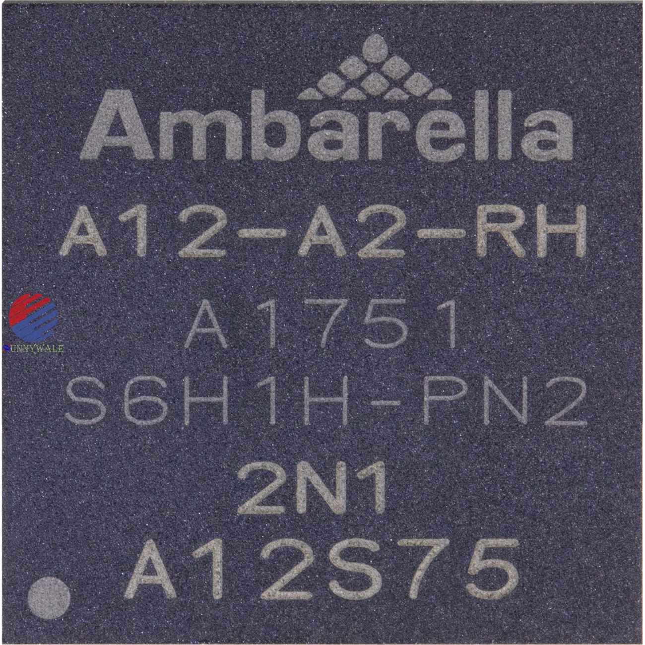
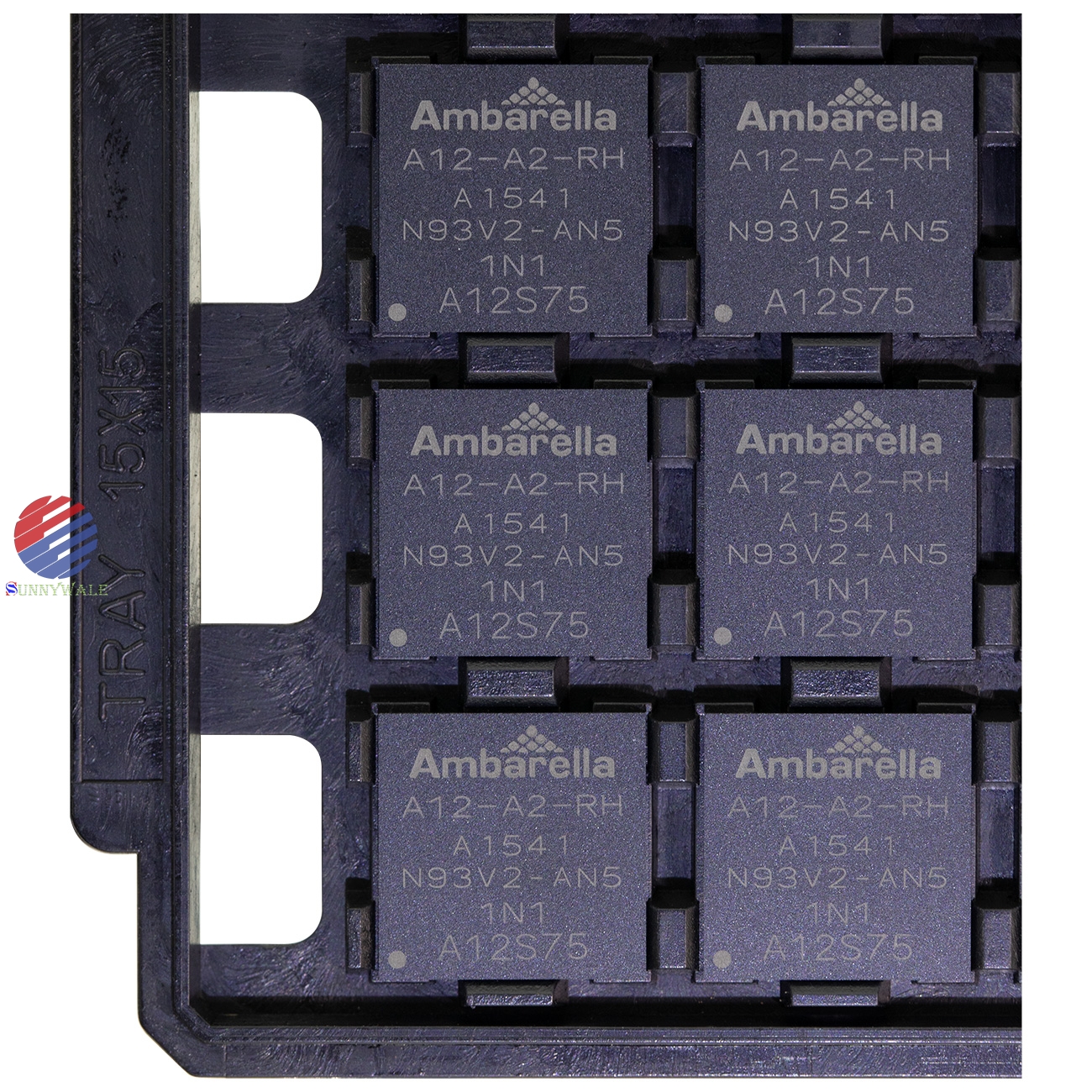
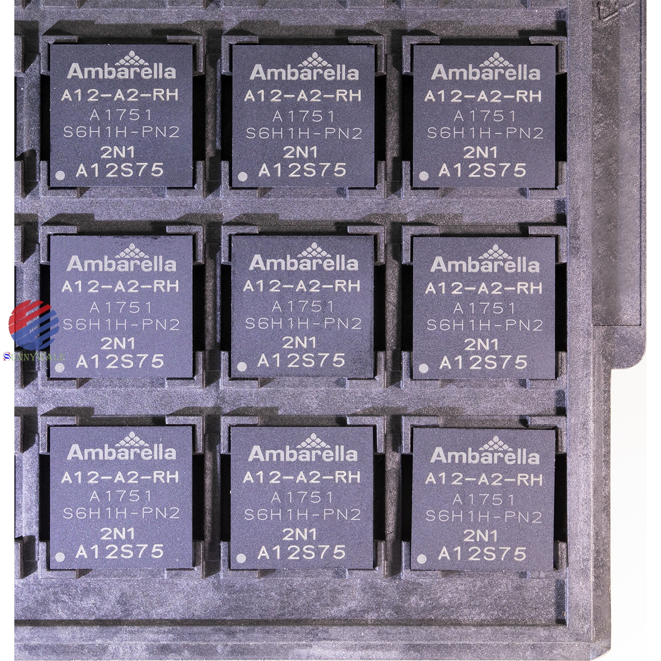
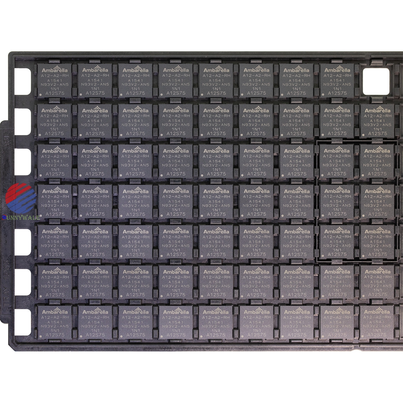
All of the above pictures are taken after matting the online showing, what you see is what you get.
Click or copy the link to browser free download the A12S75 datasheet PDF file (If you need to unlock the password, contact webmaster Wechat: 9308762).
Freight is free when you buy 2 pieces in China, if you have A12S75 inventory, you can sell to me, if you need buy A12S75, you can ask me to buy.
If you want to know about similar products
A12A75, or click here,or Visit The official website:
sunnywale.com,Search the keywod“
AMBARELLA”,it can show more details.
For more details and HD images, please copy the following link to open in your browser to view our official website;or visit our official website:
Sunnywale.com , searching keyword "
AMBARELLA".
For more details, please click
中文版