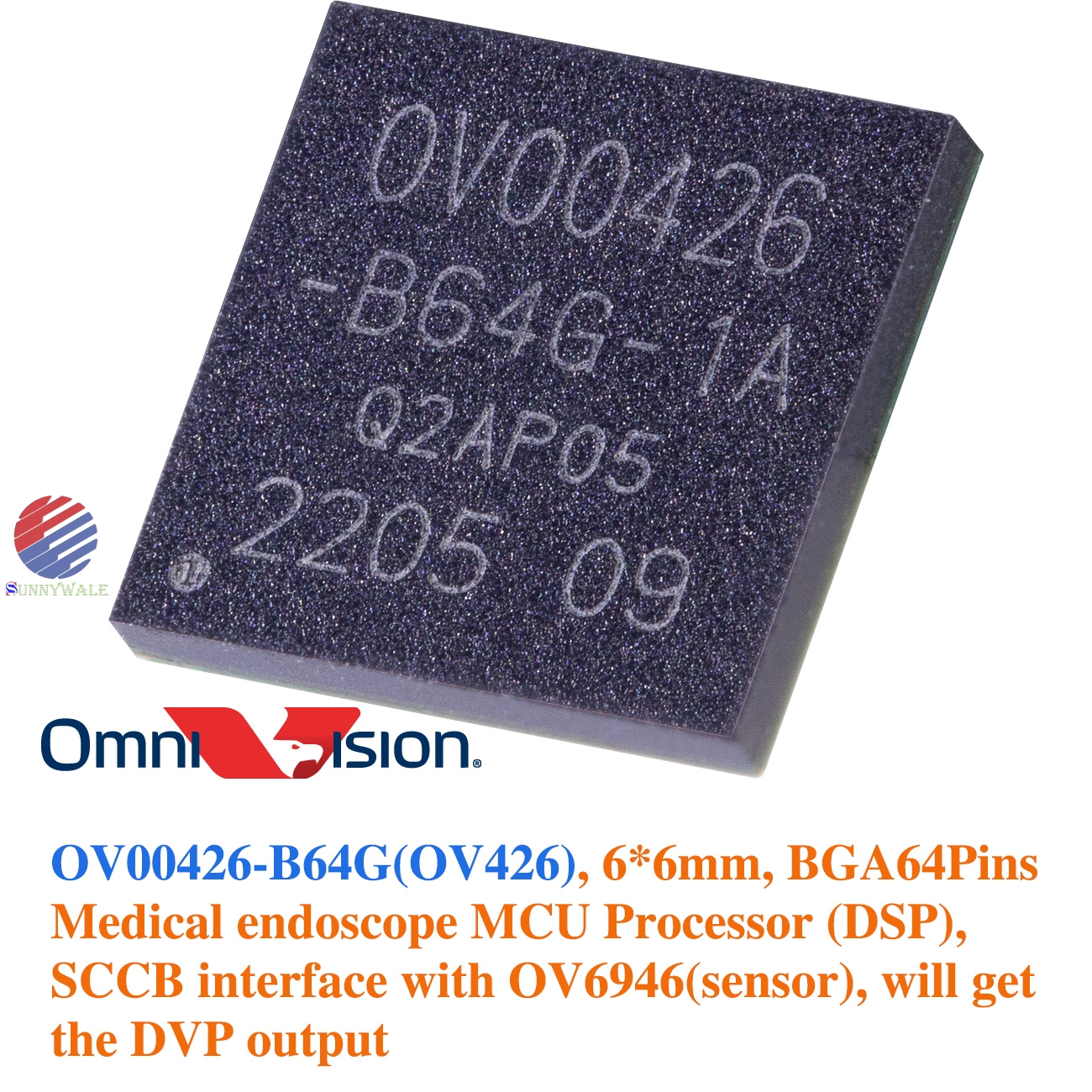
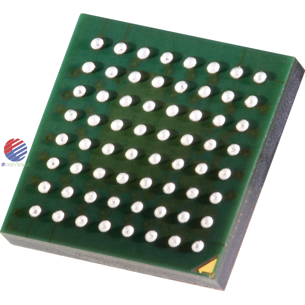
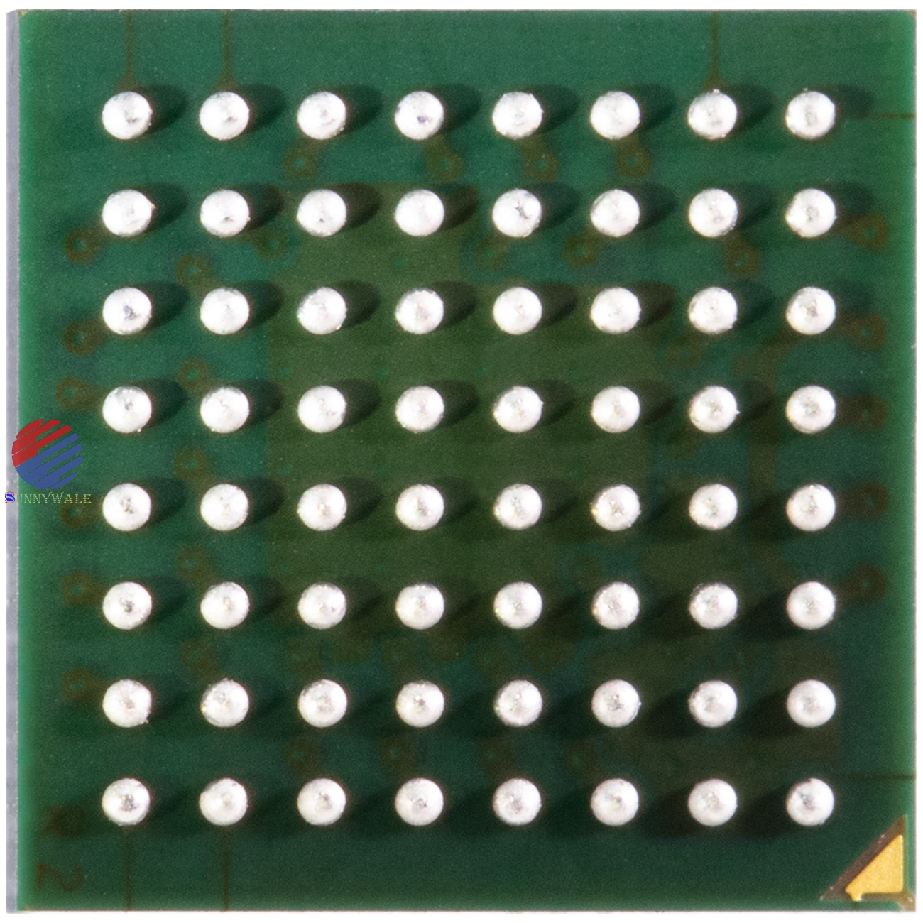
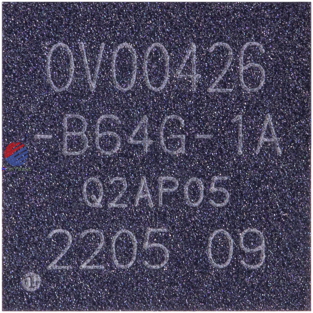
OV00426(OV426)-B64G, medical endoscope MCU DSP, with OVM6946 module, form DVP output 400x400@30fps video
2023-12-26 18:55:38
Buy Now
OV00426(OV426)-B64G, medical endoscope MCU DSP,OVM6946 supporting chip,DVP output 400x400@30fps

Features
■ complete imaging front-end solution
■ 400 x 400 at 30 fps
■ support for the following ISP functions: ADC, BLC, AEC/AGC, and MWB
■ analog input
■ support for SCCB control,10-bit DVP data output, And SPI master
■ flexible input clock
■ external system clock or independent crystal; internal PLL
■ low voltage operation
■ 6 x 6 mm to fit into handle or at back-end, near ISP in medical endoscope and other video devices
Applications
■ endoscopes
■ wearables
Key specifications
■ power supply:
¤ core: 1.5V
¤ I/O: 3.3V
¤ analog: 3.3V
■ temperature range: -30°C to 70°C
■ package dimensions: 6 mm x 6 mm
2 System level description
2.1 Overview
The OV426 is a single chip solution for the OV426 medical application. When the OV426 is combined with the OV6946,
the OV6946 provides an integrated analog-to-digital data conversion using a built-in A/D converter (ADC), black level
calibration (BLC), AEC/AGC and a final digital video parallel output (DVP). As shown in figure 2-1, the OV426 provides
a standard SCCB interface to communicate with the system and manipulate the above mentioned functions.
During operation, the OV426 synchronizes the analog output from the OV6946 through an ADC by a predefined
communication protocol. The generated digital signals will then be processed by a digital signal processor (DSP). Then
finally, standard DVP outputs are sent out.
2.2 Functional block description
2.2.1 camera interface
The analog input interface supports a bandwidth up to 8 MHz, which is two times the input clock frequency (4 MHz) in
the OV6946.
2.2.2 Reset
The OV426 clears all registers and resets them to their default values when system is powered on. A reset can also be
initiated through the SCCB interface by setting register 0x0103[0] to high. Reset requires ~2ms settling time.
The power on reset is generated internally after core power becomes stable.
2.2.3 Black level calibration
The OV426 uses black pixel data from the OV6946 to perform calibration.
2.2.4 AEC/AGC
When the AEC/AGC of the OV426 is disabled, the OV426 can manually control the exposure/gain of the OV6946.
2.2.5 SCCB slave interface
OV426 operation is controlled via the SCCB interface. The OV426 is considered to be the SCCB ’slave’ when the user
writes or reads the registers of the OV426. The OV426 slave SCCB ID is preset to 0x6C for write and 0x6D for read.
2.2.6 SCCB master interface
The user can write or read the registers of the OV6946 through the OV00426 SCCB master interface.
2.2.7 Phase-locked loop (PLL)
The internal PLL is used for synchronous clocking and may be enabled or disabled as needed.
All of the above pictures are taken after matting the online showing, what you see is what you get.
Click or copy the link to browser free download the OV426 datasheet PDF file.
Freight is free when you buy 2 pieces in China, if you have OV00426 inventory, you can sell to me, if you need buy OV00426, you can ask me to buy.
If you want to know about similar products ovm6946,
OAH428,OAH0428,OAH00428 or click here,or Visit The official website:
sunnywale.com,Search the keywods“ovm6946”,it can show more details.
If you want to read the introduction in English, please Clict the
中文版
