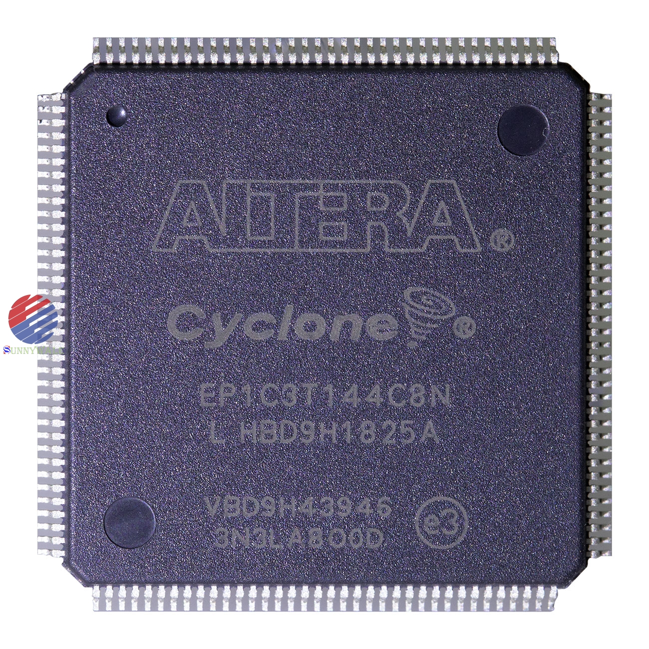
EP1C3T144C8N ALTERA Cyclone field programmable gate array, car four-wheel positioning instrument camer FPGA
2023-05-24 12:44:13
Buy Now
EP1C3T144C8N, ALTERA FPGA, ALTERA Cyclone FPGA, field programmable gate array, vehicle four-wheel locator camera FPGA
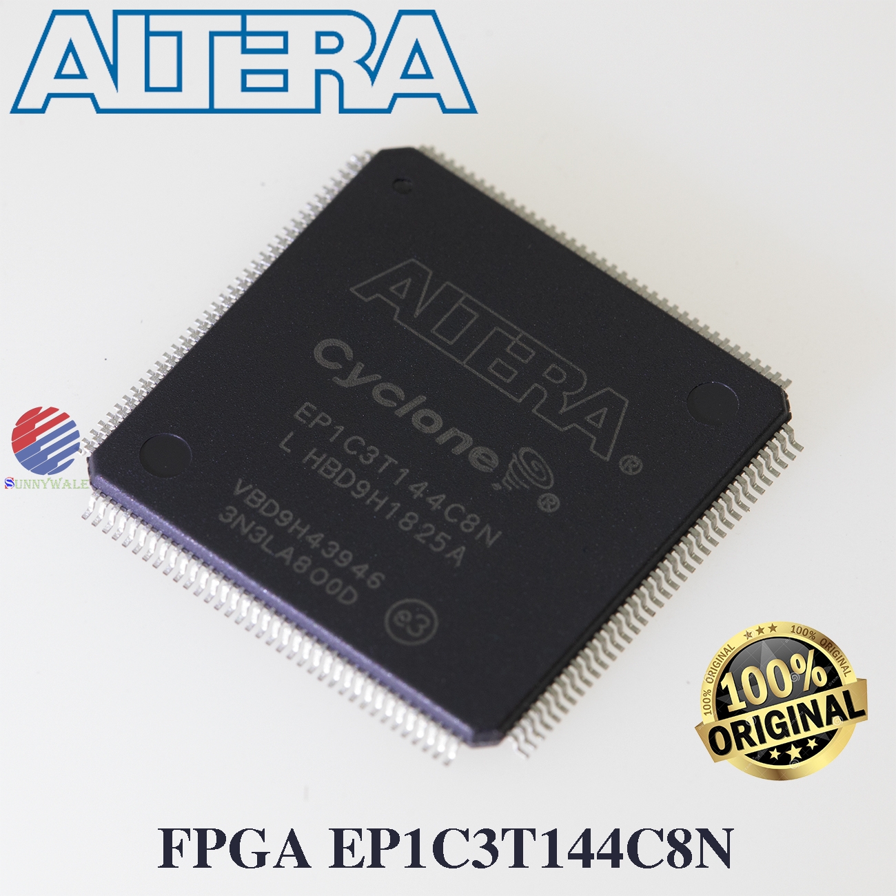
EP1C3T144C8N Introduction
Preliminary Information
The CycloneTM field programmable gate array family is based on a 1.5-V, 0.13-μm, all-layer copper SRAM process, with densities up to 20,060 logic elements (LEs) and up to 288 Kbits of RAM. With features like phaselocked loops (PLLs) for clocking and a dedicated double data rate (DDR) interface to meet DDR SDRAM and fast cycle RAM (FCRAM) memory requirements, Cyclone devices are a cost-effective solution for data-path applications. Cyclone devices support various I/O standards, including LVDS at data rates up to 311 megabits per second (Mbps) and 66-MHz, 32-bit peripheral component interconnect (PCI), for interfacing with and supporting ASSP and ASIC devices. Altera also offers new low-cost serial configuration devices to configure Cyclone devices.
Features...
■ 2,910 to 20,060 LEs, see Table 1
■ Up to 294,912 RAM bits (36,864 bytes)
■ Supports configuration through low-cost serial configuration device
■ Support for LVTTL, LVCMOS, SSTL-2, and SSTL-3 I/O standards
■ Support for 66-MHz, 32-bit PCI standard
■ Low speed (311 Mbps) LVDS I/O support
■ Up to two PLLs per device provide clock multiplication and phase shifting
■ Up to eight global clock lines with six clock resources available per logic array block (LAB) row
■ Support for external memory, including DDR SDRAM (133 MHz), FCRAM, and single data rate (SDR) SDRAM
■ Support for multiple intellectual property (IP) cores, including Altera(TM) MegaCore(TM) functions and Altera Megafunctions Partners Program (AMPPSM) megafunctions
Functional
Description
Cyclone devices contain a two-dimensional row- and column-based architecture to implement custom logic. Column and row interconnects of varying speeds provide signal interconnects between LABs and embedded memory blocks.
The logic array consists of LABs, with 10 LEs in each LAB. An LE is a small unit of logic providing efficient implementation of user logic functions. LABs are grouped into rows and columns across the device. Cyclone devices range between 2,910 to 20,060 LEs.
M4K RAM blocks are true dual-port memory blocks with 4K bits of memory plus parity (4,608 bits). These blocks provide dedicated true dual-port, simple dual-port, or single-port memory up to 36-bits wide at up to 200 MHz. These blocks are grouped into columns across the device in between certain LABs. Cyclone devices offer between 60 to 288 Kbits of embedded RAM.
Each Cyclone device I/O pin is fed by an I/O element (IOE) located at the ends of LAB rows and columns around the periphery of the device. I/O pins support various single-ended and differential I/O standards, such as the 66-MHz, 32-bit PCI standard and the LVDS I/O standard at up to 311 Mbps. Each IOE contains a bidirectional I/O buffer and three registers for registering input, output, and output-enable signals. Dual-purpose DQS, DQ, and DM pins along with delay chains (used to phase-align DDR signals) provide interface support with external memory devices such as DDR SDRAM, and FCRAM devices at up to 133 MHz (266 Mbps).
Cyclone devices provide a global clock network and up to two PLLs. The global clock network consists of eight global clock lines that drive throughout the entire device. The global clock network can provide clocks for all resources within the device, such as IOEs, LEs, and memory blocks. The global clock lines can also be used for control signals. Cyclone PLLs provide general-purpose clocking with clock multiplication and phase shifting as well as external outputs for high-speed differential I/O support.
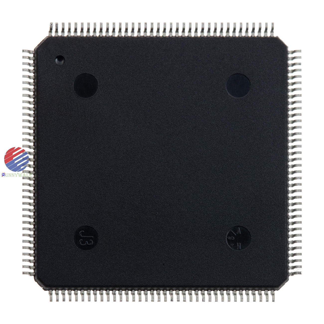
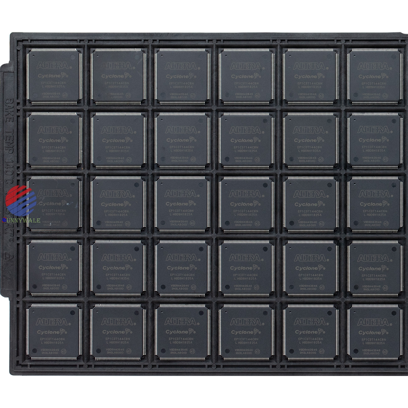
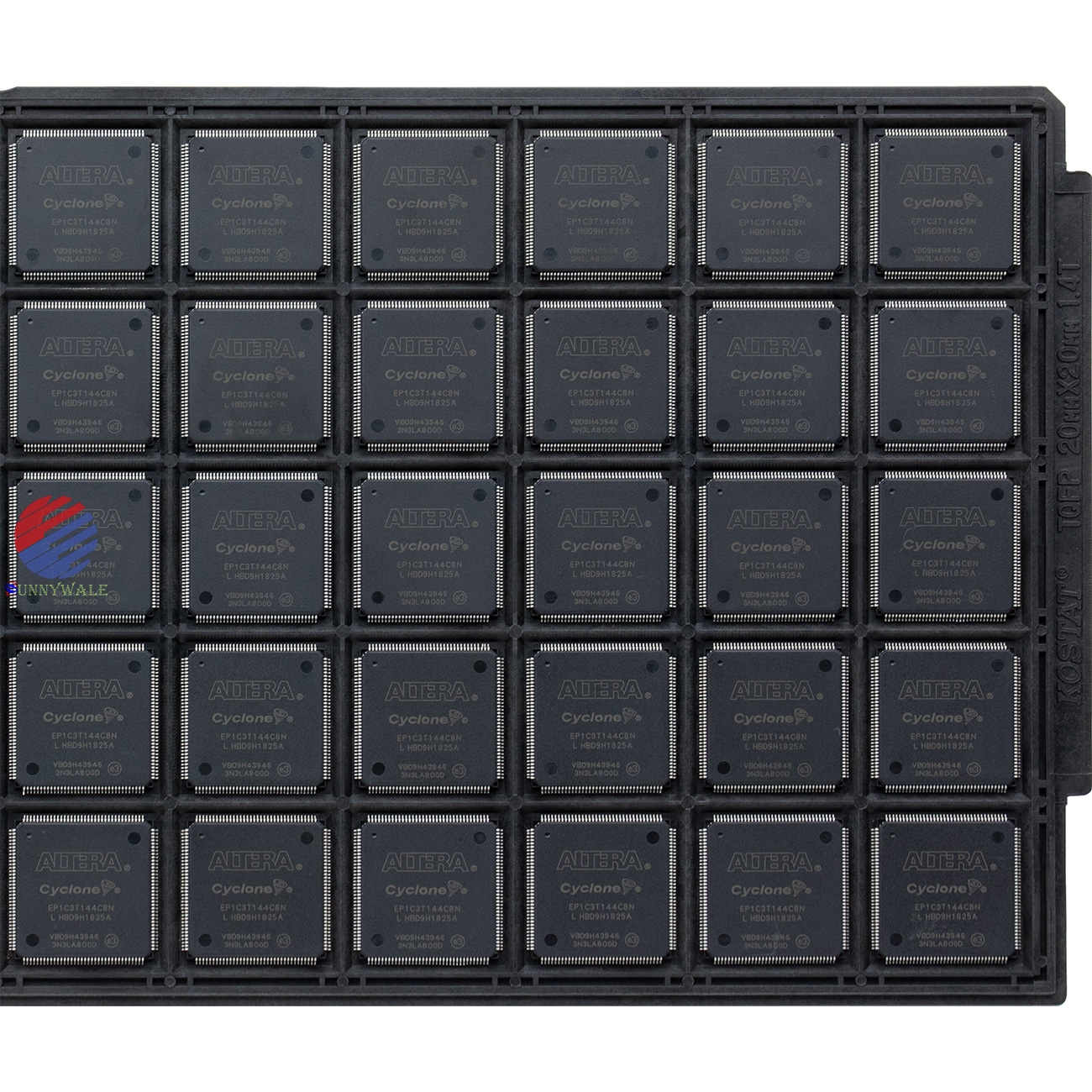
All of the above pictures are taken after matting the online showing, what you see is what you get.
Click or copy the link to free download the EP1C3T144C8N datasheet PDF file.
Freight is free when you buy 2 pieces in China, if you have EP1C3T144C8N inventory, you can sell to me, if you need buy EP1C3T144C8N, you can ask me to buy.
If you want to know about similar products FPGA, or click here,or Visit The official website:
sunnywale.com,Search the keywods“FPGA”,it can show more details.
For more details and HD images, please copy the following link to open in your browser to view our official website;or visit our official website:
en.Sunnywale.com , searching keyword "PFGA".
If you want to read the introduction in English, please Clict the
中文版