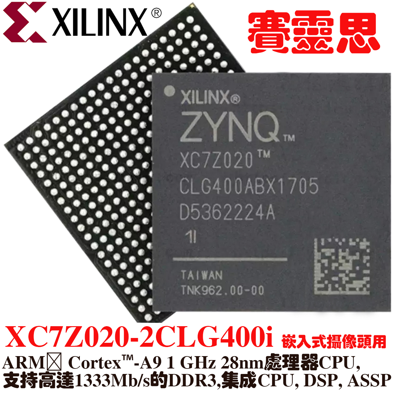
XC7Z020-2CLG400i Xilinx 单核ARM® Cortex™-A9 1 GHz 28nm处理器CPU,支持高达1333Mb/s的DDR3,集成CPU, DSP, ASSP,嵌入式摄像头用CPU
Zynq-7000 SoC Data Sheet: Overview
DS190 (v1.11.1) July 2, 2018
Product Specification
Zynq-7000 SoC First Generation Architecture
The Zynq®-7000 family is based on the Xilinx SoC architecture. These products integrate a feature-rich dual-core or single-core ARM® Cortex™-A9 based processing system (PS) and 28 nm Xilinx programmable logic (PL) in a single device. The ARM Cortex-A9 CPUs are the heart of the PS and also include on-chip memory, external memory interfaces, and a rich set of peripheral connectivity interfaces.
Processing System (PS)
ARM Cortex-A9 Based
Application Processor Unit (APU)
• 2.5 DMIPS/MHz per CPU
• CPU frequency: Up to 1 GHz
• Coherent multiprocessor support
• ARMv7-A architecture
•TrustZone® security
•Thumb®-2 instruction set
• Jazelle® RCT execution Environment Architecture•NEON™ media-processing engine
• Single and double precision Vector Floating Point Unit (VFPU)
• CoreSight™ and Program Trace Macrocell (PTM)
• Timer and Interrupts
•Three watchdog timers
•One global timer
•Two triple-timer counters
Caches
• 32 KB Level 1 4-way set-associative instruction and data caches (independent for each CPU)
• 512 KB 8-way set-associative Level 2 cache(shared between the CPUs)
• Byte-parity support
On-Chip Memory
• On-chip boot ROM
• 256 KB on-chip RAM (OCM)
• Byte-parity support
External Memory Interfaces
• Multiprotocol dynamic memory controller
• 16-bit or 32-bit interfaces to DDR3, DDR3L, DDR2, or LPDDR2 memories
• ECC support in 16-bit mode
• 1GB of address space using single rank of 8-, 16-, or 32-bit-wide memories
• Static memory interfaces
•8-bit SRAM data bus with up to 64 MB support
•Parallel NOR flash support
•ONFI1.0 NAND flash support (1-bit ECC)
•1-bit SPI, 2-bit SPI, 4-bit SPI (quad-SPI), or two quad-SPI (8-bit) serial NOR flash
8-Channel DMA Controller
•Memory-to-memory, memory-to-peripheral, peripheral-to-memory and scatter-gather transaction support
I/O Peripherals and Interfaces
•Two 10/100/1000 tri-speed Ethernet MAC peripherals with IEEE Std 802.3 and IEEE Std 1588 revision 2.0 support
•Scatter-gather DMA capability
•Recognition of 1588 rev. 2 PTP frames
•GMII, RGMII, and SGMII interfaces
• Two USB 2.0 OTG peripherals, each supporting up to 12 Endpoints
•USB 2.0 compliant device IP core
•Supports on-the-go, high-speed, full-speed, and low-speed modes
•Intel EHCI compliant USB host
•8-bit ULPI external PHY interface
• Two full CAN 2.0B compliant CAN bus interfaces
•CAN 2.0-A and CAN 2.0-B and ISO 118981-1 standard compliant
•External PHY interface
• Two SD/SDIO 2.0/MMC3.31 compliant controllers
• Two full-duplex SPI ports with three peripheral chip selects
• Two high-speed UARTs (up to 1 Mb/s)
• Two master and slave I2C interfaces
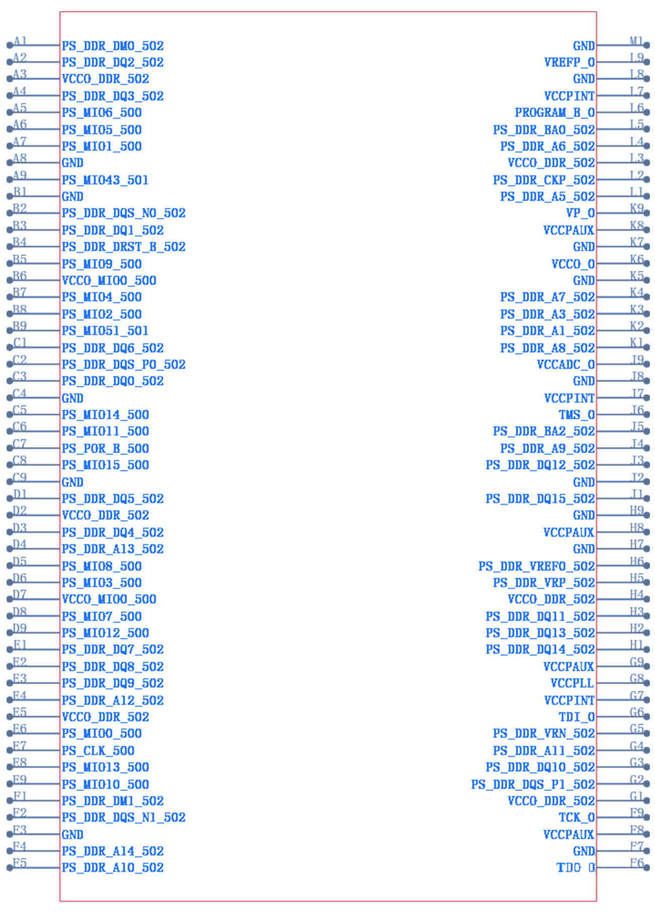
• GPIO with four 32-bit banks, of which up to 54 bits can be used with the PS I/O (one bank of 32b and one bank of 22b) and up to 64 bits (up to two banks of 32b) connected to the Programmable Logic
• Up to 54 flexible multiplexed I/O (MIO) for peripheral pin assignments
Interconnect
• High-bandwidth connectivity within PS and between PS and PL
• ARM AMBA® AXI based
• QoS support on critical masters for latency and bandwidth control
Programmable Logic (PL)
Configurable Logic Blocks (CLB)
• Look-up tables (LUT)
• Flip-flops
• Cascadeable adders
36 Kb Block RAM
• True Dual-Port
• Up to 72 bits wide
• Configurable as dual 18 Kb block RAM
DSP Blocks
• 18 x 25 signed multiply
• 48-bit adder/accumulator
• 25-bit pre-adder
Programmable I/O Blocks
• Supports LVCMOS, LVDS, and SSTL
• 1.2V to 3.3V I/O
• Programmable I/O delay and SerDe
JTAG Boundary-Scan
• IEEE Std 1149.1 Compatible Test Interface
PCI Express® Block
• Supports Root complex and End Point configurations
• Supports up to Gen2 speeds
• Supports up to 8 lanes
Serial Transceivers
• Up to 16 receivers and transmitters
• Supports up to 12.5 Gb/s data rates
Two 12-Bit Analog-to-Digital Converters
• On-chip voltage and temperature sensing
• Up to 17 external differential input channels
• One million samples per second maximum conversion rat
Zynq-7000 Family Description
The Zynq-7000 family offers the flexibility and scalability of an FPGA, while providing performance, power, and ease of use typically associated with ASIC and ASSPs. The range of devices in the Zynq-7000 family allows designers to target cost-sensitive as well as high-performance applications from a single platform using industry-standard tools. While each device in the Zynq-7000 family contains the same PS, the PL and I/O resources vary between the devices. As a result, the Zynq-7000 and Zynq-7000S SoCs are able to serve a wide range of applications including:
• Automotive driver assistance, driver information, and infotainment
• Broadcast camera
• Industrial motor control, industrial networking, and machine vision
• IP and Smart camera
• LTE radio and baseband
• Medical diagnostics and imaging
• Multifunction printers
• Video and night vision equipment
The Zynq-7000 architecture enables implementation of custom logic in the PL and custom software in the PS. It allows for the realization of unique and differentiated system functions. The integration of the PS with the PL allows levels of performance that two-chip solutions (e.g., an ASSP with an FPGA) cannot match due to their limited I/O bandwidth, latency, and power budgets.
Xilinx offers a large number of soft IP for the Zynq-7000 family. Stand-alone and Linux device drivers are available for the peripherals in the PS and the PL. The Vivado® Design Suite development environment enables a rapid product development for software, hardware, and systems engineers. Adoption of the ARM-based PS also brings a broad range of third-party tools and IP providers in combination with Xilinx’s existing PL ecosystem.
The inclusion of an application processor enables high-level operating system support, e.g., Linux. Other standard operating systems used with the Cortex-A9 processor are also available for the Zynq-7000 family.The PS and the PL are on separate power domains, enabling the user of these devices to power down the PL for power management if required. The processors in the PS always boot first, allowing a software centric approach for PL configuration. PL configuration is managed by software running on the CPU, so it boots similar to an ASSP.
Zynq-7000 SoC数据表:概述
DS190 (v1.11.1) 2018年7月2日
产品规格
Zynq-7000 SoC第一代架构
Zynq®-7000系列基于Xilinx SoC架构。这些产品集成了功能丰富的双核或单核ARM®Cortex™-A9处理系统(PS)和28 nm Xilinx可编程逻辑(PL)在单个设备。ARM Cortex-A9 cpu是PS的核心,还包括片上内存、外部内存接口和一组丰富的外围连接接口。
处理系统(PS)
基于ARM cortex - A9 应用处理器单元(APU)
• 每个CPU 2.5 DMIPS/MHz
• CPU频率:高达1ghz
• 相干多处理器支持
• ARMv7-A架构
• TrustZone®安全
• 拇指®2指令集
• NEON™媒体处理引擎
• 单精度和双精度矢量浮点单元(VFPU)
• CoreSight™和程序跟踪Macrocell (PTM)
• 定时器和中断
• 三个看门狗定时器
• 一个全球计时器
• 两个triple-timer计数器
缓存
• 32 KB 1级4路集关联指令和数据缓存(独立于每个CPU)
• 512kb 8路设置关联二级缓存(在cpu之间共享)
• Byte-parity支持
片上存储器
• 芯片上的引导ROM
• 256kb芯片内RAM (OCM)
• Byte-parity支持
外部存储器接口
• 多协议动态内存控制器
• 16位或32位接口,支持DDR3、DDR3L、DDR2或LPDDR2内存
• 16位模式下的ECC支持
• 1GB的地址空间使用单秩8,16,或32位宽内存
• 静态内存接口
• 8位SRAM数据总线,支持高达64 MB
• 并行NOR闪存支持
• ONFI1.0 NAND flash支持(1位ECC)
• 1位SPI, 2位SPI, 4位SPI (quad-SPI),或两个quad-SPI(8位)串行NOR flash
8-Channel DMA 控制器
•内存到内存、内存到外设、外设到内存和散集事务支持
I/O外设和接口
• 两个10/100/1000三速以太网MAC外设,支持IEEE标准802.3和IEEE标准1588修订版2.0
• 散集DMA功能
• 识别1588修订版2 PTP帧
• GMII、RGMII和SGMII接口
•两个usb2.0 OTG外设,每个支持多达12个端点
• USB 2.0兼容的设备IP核
• 支持on- go、高速、全速和低速模式
• Intel EHCI兼容USB主机
• 8位ULPI外部PHY接口
• 两个完全符合CAN 2.0B总线接口
• 符合CAN 2.0-A、CAN 2.0-B和ISO 118981-1标准
• 外部PHY接口
2个兼容SD/SDIO 2.0/MMC3.31的控制器
• 两个全双工SPI端口与三个外围芯片选择
• 两个高速UARTs(高达1mb /s)
• 两个主人和奴隶I2C接口
• GPIO 4个32位的银行,其中多达54位可以使用PS I / O (32 b的一个银行和一个银行22 b)和64位(两家银行的32 b)连接到可编程逻辑
• 多达54个灵活的多路I / O(绪)外围销作业
互连
• PS内部和PS与PL之间的高带宽连接
• 基于ARM AMBA®AXI
• 对关键主机的QoS支持,用于延迟和带宽控制
可编程序逻辑(PL)
可配置逻辑块(CLB)
• 查找表(LUT)
• 人字拖
• Cascadeable加法器
36kb块RAM
• 真正的双端口
• 高达72位宽
• 可配置为双18kb块RAM
DSP模块
• 18 × 25有符号的乘法
• 48比特位加法器/蓄电池
• 25-bit公元前由
可编程I / O模块
• 支持LVCMOS、LVDS、SSTL
• 1.2V至3.3V I/O
• 可编程I/O延迟和SerDe
JTAG边界
IEEE标准1149.1兼容测试接口
PCI Express®块
• 支持根复杂和端点配置
• 最大支持Gen2速度
• 最多支持8个通道
串行收发器
• 多达16个接收器和发射器
• 支持高达12.5 Gb/s的数据速率
两个12位模数转换器
• 片上电压和温度传感
• 多达17个外部差分输入通道
• 每秒100万个样品的最大转换鼠
zynq - 7000系列描述
Zynq-7000系列提供了FPGA的灵活性和可扩展性,同时提供了通常与ASIC和ASSPs相关的性能、功耗和易用性。Zynq-7000系列设备允许设计师使用行业标准工具,在一个平台上针对成本敏感和高性能的应用程序。虽然Zynq-7000家族中的每个设备都包含相同的PS,但PL和I/O资源在不同设备之间是不同的。因此,Zynq-7000和Zynq-7000S soc能够提供广泛的应用,包括:
• 汽车驾驶员辅助、驾驶员信息和信息娱乐
• 广播相机
• 工业电机控制、工业网络和机器视觉
• IP和智能摄像头
• LTE无线电和基带
• 医疗诊断和成像
• 多功能打印机
• 视频和夜视设备
Zynq-7000体系结构允许在PL中实现自定义逻辑,在PS中实现自定义软件。它允许实现独特和差异化的系统功能。PS与PL的集成允许双芯片解决方案(例如,带有FPGA的ASSP)无法匹配的性能水平,因为它们有限的I/O带宽、延迟和功耗预算。
Xilinx为Zynq-7000系列提供了大量的软IP。独立和Linux设备驱动程序可用于PS和PL中的外设。Vivado®Design Suite开发环境可以为软件、硬件和系统工程师提供快速的产品开发。采用基于arm的PS还带来了广泛的第三方工具和IP提供商,并结合Xilinx现有的PL生态系统。
应用程序处理器的包含使高级操作系统支持成为可能,例如Linux。其他与Cortex-A9处理器一起使用的标准操作系统也可用于Zynq-7000系列。PS和PL位于不同的电源域,允许这些设备的用户在需要时关闭PL进行电源管理。PS中的处理器总是首先引导,允许以软件为中心的PL配置方法。PL配置由运行在CPU上的软件管理,因此它的引导类似于ASSP。
参数列表
技术参数:针脚数400,RAM大小256 KB
封装参数:引脚数400
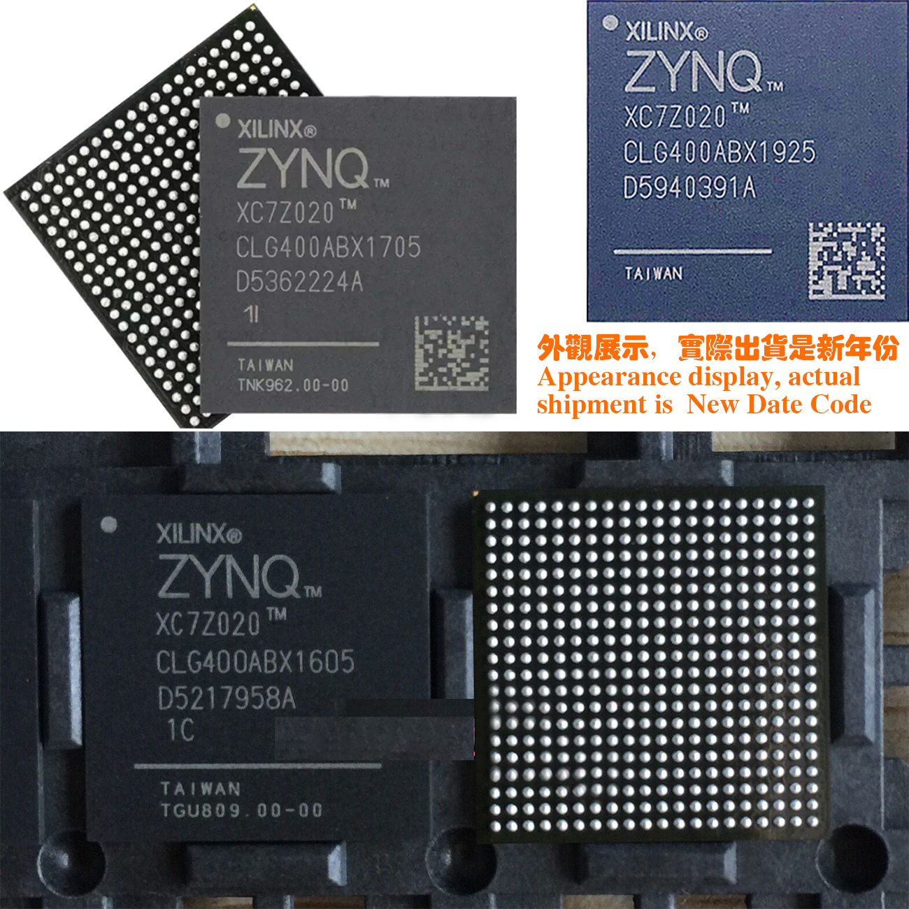
封装:CSPBGA-400
物理参数:工作温度-40℃ ~ 100℃ (TJ)
产品生命周期:Active
包装方式:Tray
符合标准:RoHS标准RoHS Compliant
含铅标准:Lead Free
IC SOC CORTEX-A9 766MHZ 400BGA
MPU Zynq-7000 Thumb-2 32-Bit 733MHz 1.2V/3.3V 400-Pin CS-BGA
DeviceMart: IC SOC CORTEX-A9 ARTIX-7 400BGA
产品概述
MPU Zynq-7000 Thumb-2 32Bit 733MHz 1.2V/3.3V 400Pin CS-BGA
Xilinx Zynq®-7000 All Programmable SoC (AP SoC)系列将集成了基于ARM®处理器的软件可编程性与FPGA的硬件可编程性, 可在单个器件上集成CPU, DSP, ASSP与混合信号功能, 从而实现关键分析与硬件加速. 可选单核Zynq®-7000S与双核Zynq®-7000器件. Zynq®-7000S器件具有单核ARM® Cortex™-A9处理器, 连接基于28nm Artix®-7的可编程逻辑, 代表了可扩展Zynq®-7000平台的最低成本起点. 非常适合工业物联网应用, 如电机控制与嵌入式视觉应用. Zynq®-7000器件配备双核ARM®Cortex™-A9处理器, 集成了基于28nm Artix®-7或Kintex®-7的可编程逻辑 (高达6.6M逻辑逻辑单元与12.5Gb/s收发器), 拥有出色的功率性能, 最大的设计灵活性, 适用于多种嵌入式应用设计.
. 可选-3, -2, -2L, -1, -1L速度等级与商业/工业/扩展温度
. 每个CPU 2.5DMIPS/MHz, 1GHz CPU频率, ARMv7-A与Jazelle RCT执行环境架构
. NEON™媒体处理引擎, 矢量浮点计算单元, CoreSight™与程序追踪宏单元
. 32KB指令, 每处理器L1缓存32KB数据, 512KB L2缓存, 256KB片上存储器
. DDR3, DDR3L, DDR2, LPDDR2外部存储器支持, 2 x quad-SPI, NAND, NOR静态存储器支持
. 8通道DMA控制器, 2 x UART, 2 x CAN 2.0B, 2 x I2C, 2 x SPI, 4 x 32位GPIO外设
. 2 x USB 2.0 (OTG), 2 x 三模千兆以太网, 2 x SD/SDIO外设
. RSA认证, AES与SHA 256位解密与认证, 以实现安全启动.Zynq®-7000 AP SoC提供了更智能, 更优化与更安全的解决方案
. 卓越的集成性, 性能与能力, 可靠的生产力
The Xilinx XC7Z020-2CLG400i device belongs to the Zynq-7000 family and is grounded on the SoC architecture of Xilinx. The device is integrating a dual or single-core ARM Cortex processor that has rich features. The processor is grounded on the processing system and is having 28nm of programming logic. The central processing unit of the device is considered the heart of the processing system and is comprising of on-chip memory, state-of-the-art interfaces for peripheral connectivity, and interfaces for external memory too. The central processing unit has 2.5 DMIPS per MHz through each CPU with a frequency capability of 1 GHz. The device has coherent multiprocessor support, a couple of triple-timer counters, a global timer, 3 watchdog timers, and interrupts.
The device has caches of up to 32Kb of level-1 that have 4-way set-associative instructions and is independent of each CPU. There is also a 512Kb of level-2 that has 8-way set-associative instructions and is shared in between central processing units. Furthermore, the caches are having byte-parity support as well. Xilinx XC7Z020-2CLG400i has 256Kb On-Chip RAM and ROM with byte-parity support. This IC has a multi-protocol controller for dynamic memory with 32 or 16-bit interfaces for LPDDR2, DDR2, DDR3L, and DDR3 memories. The device has 16-bit support for ECC. It has an SRAM data bus of 8 bits with 64Mb support, parallels support for NOR flash, and 8 channel DMA controller capable of support for scatter-gather transactions, peripheral to memory, memory to peripheral, and memory to memory. The interconnects of the device are having a high-bandwidth connection for its PS and among PL and PS. The configurable logic block of Xilinx XC7Z020-2CLG400i has cascaded adders, flip-flops, and lookup tables. Block RAM is dual-port, expandable up to 72 bits, and can be configured in the form of dual 18Kb block RAM too. The DSP block has a pre-adder of 25-bit, accumulator or adder of 48-bit, and a signed multiplier of 18×25 bits. Its PCI block is supporting up to 8 lanes, 2nd generation speeds, along with endpoint configurations, and root complex.
Family Description of Xilinx XC7Z020-2CLG400i
The family of Xilinx XC7Z020-2CLG400i is Zynq-7000 which offers scalability and flexibility of FPGAs delivering ease of use, power, and performance usually associated with ASSPs and ASICs. The devices of this family are allowing the designers to target cost-sensitive and higher performance enabled applications through a single platform through the use of tools of industry-standard. All of the devices of the family are having identical PS but PL and input/output resources are varying in all devices. The device is utilized for a wide range of applications as in the automotive industry it has applications in driver assistance, information for drivers, and infotainment. It is used in broadcast cameras, machine vision, industrial networking, and motor control. Smart and IP cameras have also been used along with baseband and LTE radios. The device is used in biomedical imaging, diagnostics, multi-function printers, night-vision equipment, and video devices.
Memory Interfaces
The unit of memory interfaces of the Xilinx XC7Z020-2CLG400i device is comprising of controllers for dynamic and static memory interfaces. The interface for dynamic memory is supporting DDR3L, LPDDR2, DDR3, and DDR2 memories. While the interface of static memory is having support for interfaces of NOR flash, quad-SPI flash, parallel data bus, and static flash interface.
Interfaces for Dynamic Memory
The DDR memory controller which is a multi-protocol controller could be configured for delivering 32 or 16-bit broad accesses to its 1Gb address spaces through the utilization of a unity rank configuration for 8, 16, or 32-bit DRAM memories. The support for ECC is in the form of a 16-bit mode for bus access. The PS of Xilinx XC7Z020-2CLG400i is incorporating both associated PHY and DDR controllers encompassing its integrated inputs/outputs. The device is supporting up to the speed of 1333Mb/s for its DDR3 support. The DDR memory controller is multi-ported and is enabling the system processing and its programmable logic for common access to have a shared memory. There are 4 AXI slave ports in the DDR controller for this purpose. One of the 64-bit ports is having the purpose of ARM CPU through the controller of L2 cache and could be configured for lower latency. Two 64-bit ports are dedicatedly assigned to PL access. One of the 64-bit AXI ports is common for all of the AXI masters through a central interconnect.
Interfaces for Static Memory
The memory interfaces of Xilinx XC7Z020-2CLG400i for static memory are supporting external static memories. The 8-bit SRAM data bus is supporting till 64Mb, while the 8-bit NOR flash parallel data bus supports up to 64Mb. The integrated ONFI NAND flash is supporting up to 1-bit ECC. Whereas, 1, 2, and 4-bit SPI or a couple of quad-SPIs each of 8 bits are supported through serial NOR flash.
The Input / Output Peripherals of Xilinx XC7Z020-2CLG400i
The input/output peripheral unit of the device is consisting of peripherals for data communication. The key features of the unit comprise two tri-mode peripherals for Ethernet MAC having support for IEEE standard 1588 and IEEE standard 802.3. The device also has the capability of scatter-gather DMA. Xilinx XC7Z020-2CLG400i has a feature for recognition of 1588 revision for 2 PTP frames. It also supports an external PHY interface along a couple of USB 2.0 peripherals of OTG mode each having support of 12 endpoints. The device is entirely compliant with USB 2.0 standards with host and device IP core. It delivers an 8-bit external PHY interface for ULPI. It has 2 full CAN buses fully compliant to CAN 2.0B interfaces. With the utilization of its TrustZone system, 2 ethernets, 2 SDIO, and 2 USB ports are configurable in both non-secure and secure modes. The input/output peripherals are also communicating with the external devices via shared pool of 54 integrated multi-use input/output pins. Every peripheral could be assigned to either of its many pre-defined pin groups that enable flexible assignment of numerous devices on a simultaneous basis. Though all of its 54 pins are not capable to be used simultaneously for its input/output peripherals but most of its input/output interfaces for signals are available for PL to enable utilization of standard PL at input/output pins in powered ON conditions.
Xilinx XC7Z020-2CLG400i器件属于 Zynq-7000 系列,基于 Xilinx 的SoC架构。该设备集成了具有丰富功能的双核或单核ARM Cortex 处理器。该处理器基于处理系统,具有 28nm 的编程逻辑。该设备的中央处理单元被认为是处理系统的核心,由片上存储器、用于外围连接的最先进接口以及用于外部存储器的接口组成。中央处理器通过每个 CPU 具有 2.5 DMIPS/MHz,频率能力为 1 GHz。该设备具有一致的多处理器支持、几个三重定时器计数器、一个全局定时器、3 个看门狗定时器和中断。
该器件具有高达 32Kb 的 1 级高速缓存,具有 4 路组关联指令,并且独立于每个 CPU。还有一个 512Kb 的 2 级具有 8 路组关联指令并在中央处理单元之间共享。此外,缓存也支持字节奇偶校验。赛灵思 XC7Z020- 2CLG400i具有 256Kb 片上 RAM 和支持字节奇偶校验的 ROM。该 IC 具有用于动态存储器的多协议控制器,具有用于 LPDDR2、DDR2、DDR3L 和 DDR3 存储器的 32 位或 16 位接口。该器件具有对 ECC 的 16 位支持。它具有 8 位 SRAM 数据总线,支持 64Mb,并行支持 NOR 闪存,以及 8 通道 DMA 控制器,能够支持分散-聚集事务、外设到内存、内存到外设和内存到内存。该设备的互连在其 PS 以及 PL 和 PS 之间具有高带宽连接。Xilinx XC7Z020-2CLG400i的可配置逻辑块 具有级联加法器、触发器和查找表。Block RAM 是双端口的,可扩展至 72 位,也可以配置成双 18Kb Block RAM 的形式。DSP 模块有一个 25 位的预加器、一个 48 位的累加器或加法器,以及一个 18×25 位的有符号乘法器。它的 PCI 模块支持多达 8 个通道、第 2代 速度、端点配置和根复合体。
Xilinx XC7Z020-2CLG400i 系列说明
Xilinx XC7Z020-2CLG400i 系列是Zynq-7000,它提供 FPGA 的可扩展性和灵活性,提供通常与 ASSP 和 ASIC 相关的易用性、功耗和性能。该系列的器件允许设计人员通过使用行业标准工具的单一平台来瞄准成本敏感型和更高性能的应用程序。该系列的所有设备都具有相同的 PS,但 PL 和输入/输出资源在所有设备中都不同。该设备被用于广泛的应用,如在汽车它在驾驶员辅助、驾驶员信息和信息娱乐方面有应用。它用于广播摄像机、机器视觉、工业网络和电机控制。智能和 IP 摄像机也已与基带和 LTE 无线电一起使用。该设备用于生物医学成像、诊断、多功能打印机、夜视设备和视频设备。
内存接口
Xilinx XC7Z020-2CLG400i器件的存储器接口单元由 用于动态和静态存储器接口的控制器组成。动态内存接口支持 DDR3L、LPDDR2、DDR3 和 DDR2 内存。而静态存储器接口则支持NOR flash、quad- SPI flash、并行数据总线和静态flash接口。
动态内存接口
DDR 内存控制器是一种多协议控制器,可配置为通过使用 8、16 或 32 位 DRAM 内存的统一等级配置来提供对其 1Gb 地址空间的 32 或 16 位广泛访问。对 ECC 的支持以 16 位模式的形式进行总线访问。Xilinx XC7Z020-2CLG400i的PS正在整合相关的 PHY 和 DDR 控制器,包括其集成的输入/输出。该设备支持高达 1333Mb/s 的 DDR3 支持速度。DDR 内存控制器是多端口的,它使系统处理及其用于公共访问的可编程逻辑具有共享内存。为此,DDR 控制器中有 4 个 AXI 从端口。64 位端口之一是通过二级缓存控制器实现 ARM CPU 的目的,并且可以配置为降低延迟。两个 64 位端口专门分配给 PL 访问。一个 64 位 AXI 端口通过中央互连对所有 AXI 主设备都是通用的。
静态内存接口
Xilinx XC7Z020-2CLG400i用于静态存储器的存储器接口 支持外部静态存储器。8 位 SRAM 数据总线最高支持 64Mb,而 8 位 NOR 闪存并行数据总线最高支持 64Mb。集成的 ONFI NAND 闪存最多支持 1 位 ECC。然而,串行 NOR 闪存支持 1、2 和 4 位 SPI 或几个 8 位的四路 SPI。
Xilinx XC7Z020-2CLG400i的输入/输出外设