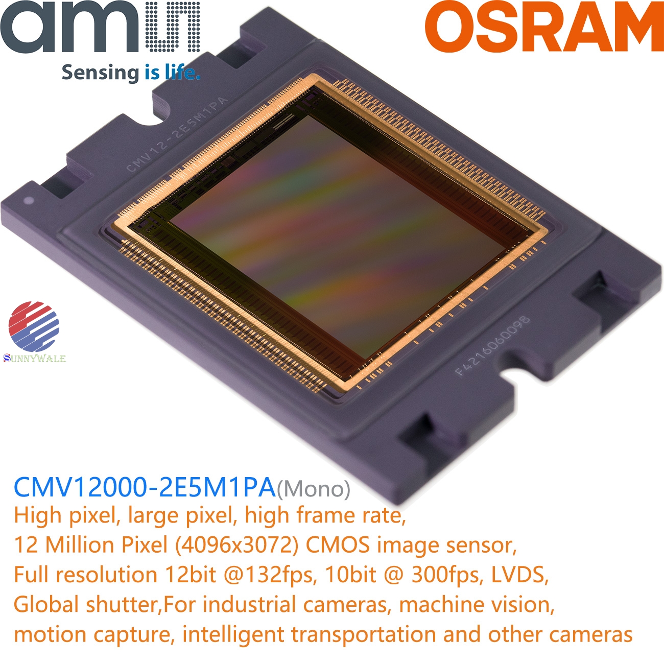
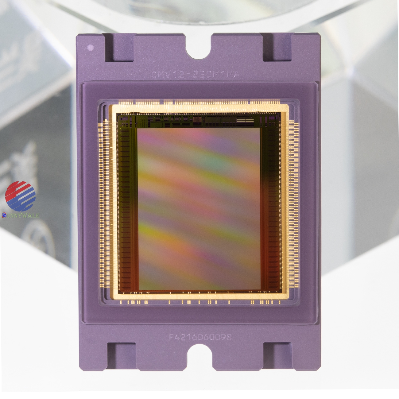
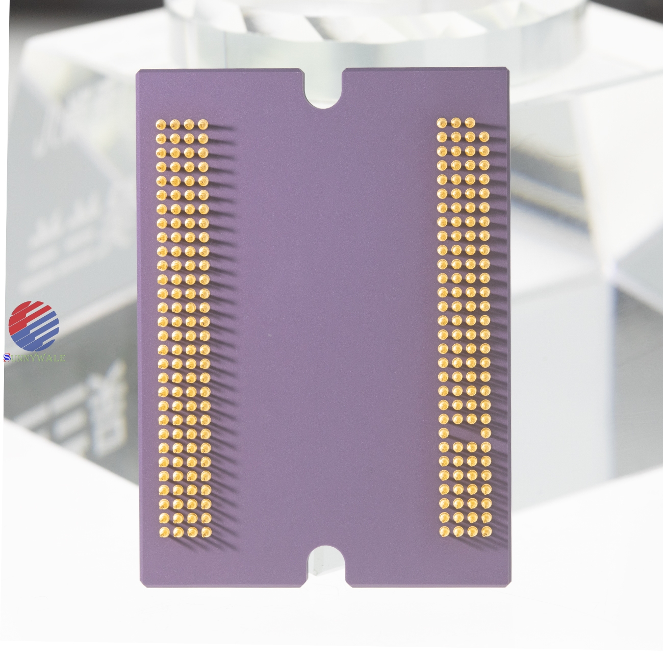
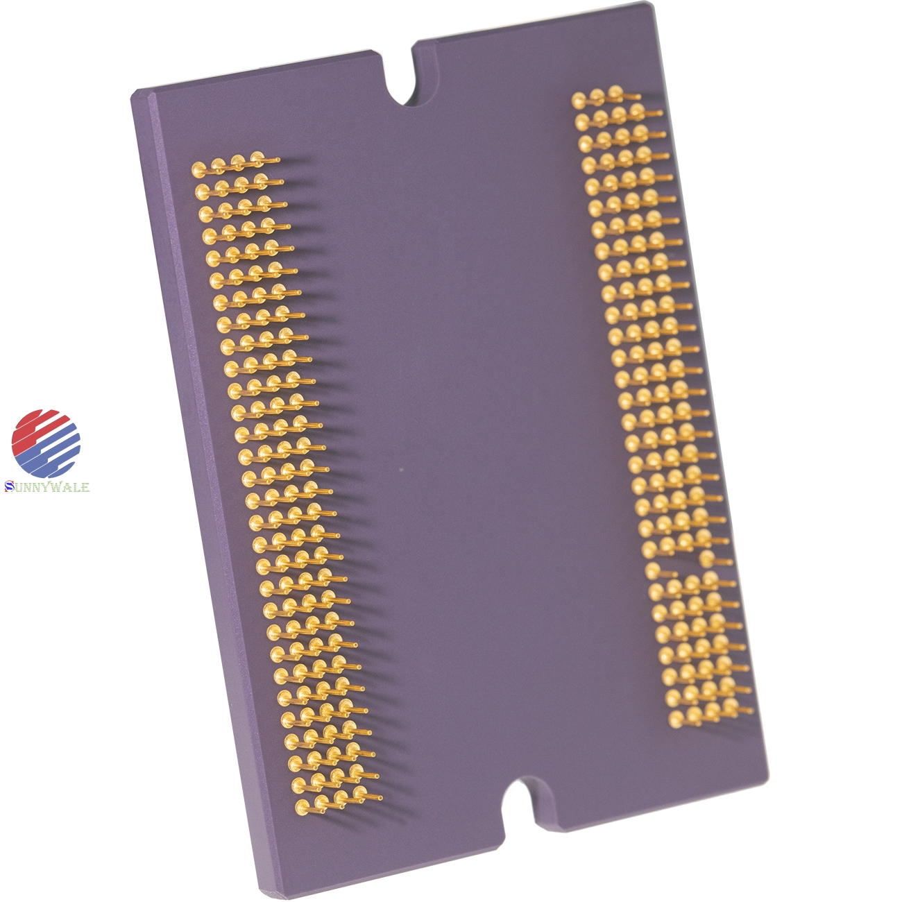
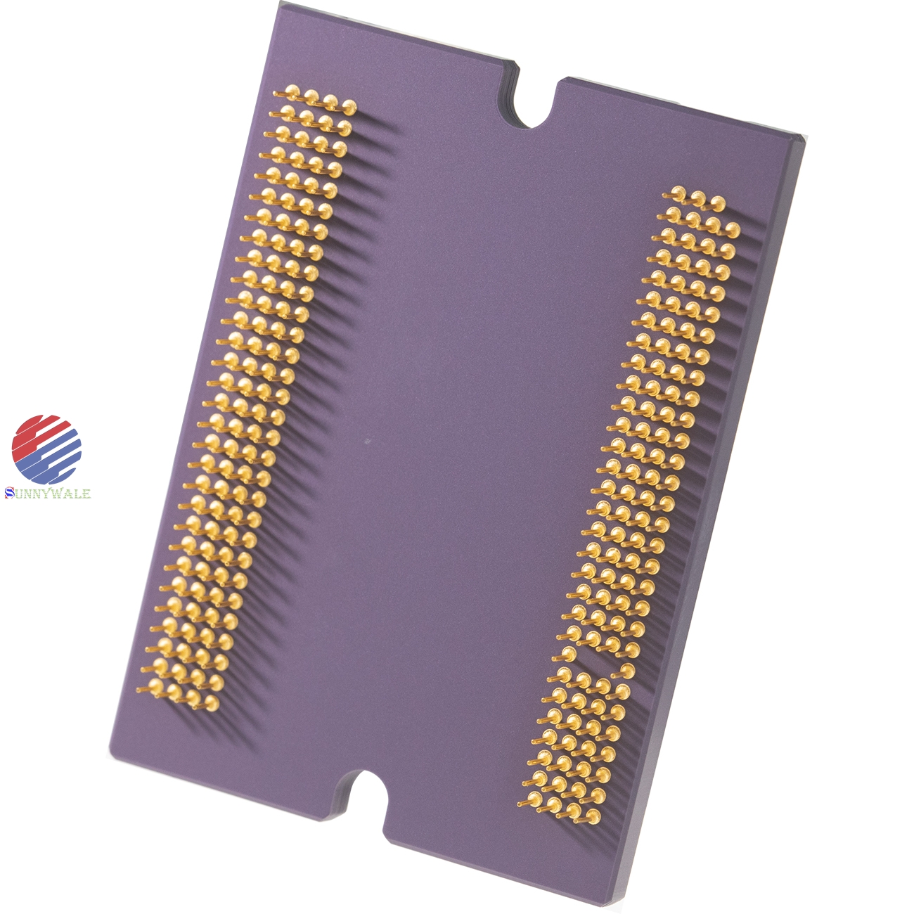
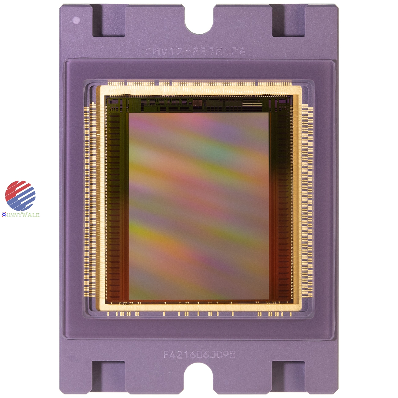
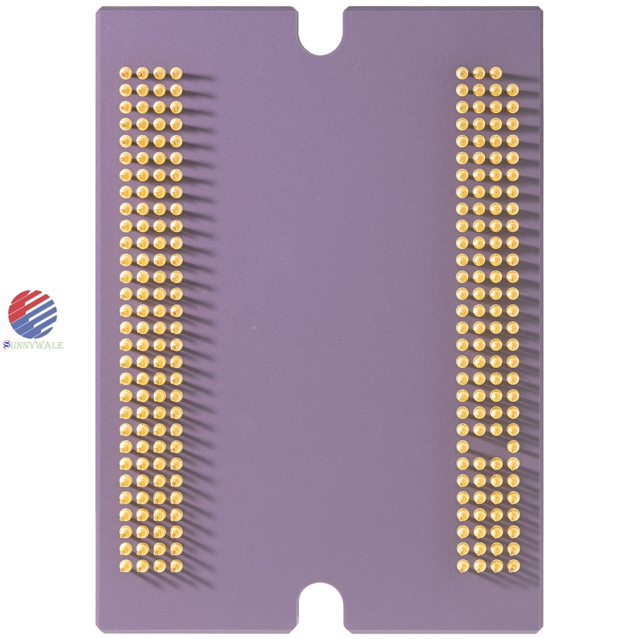
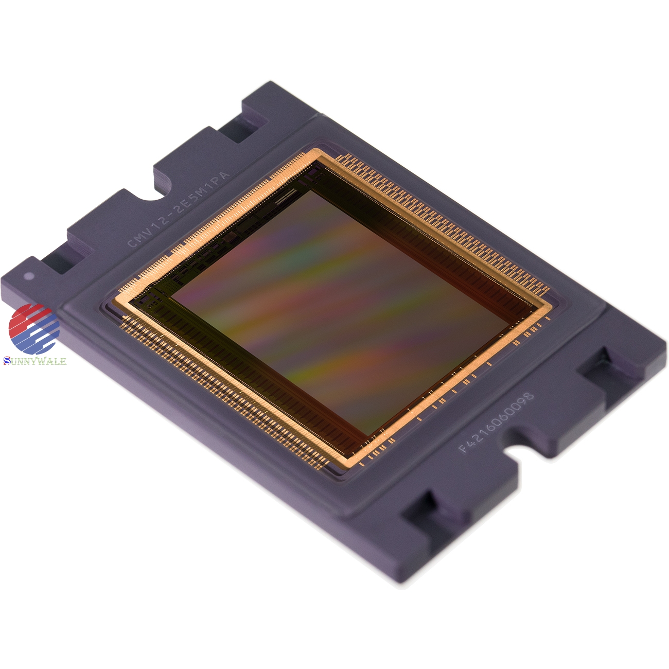
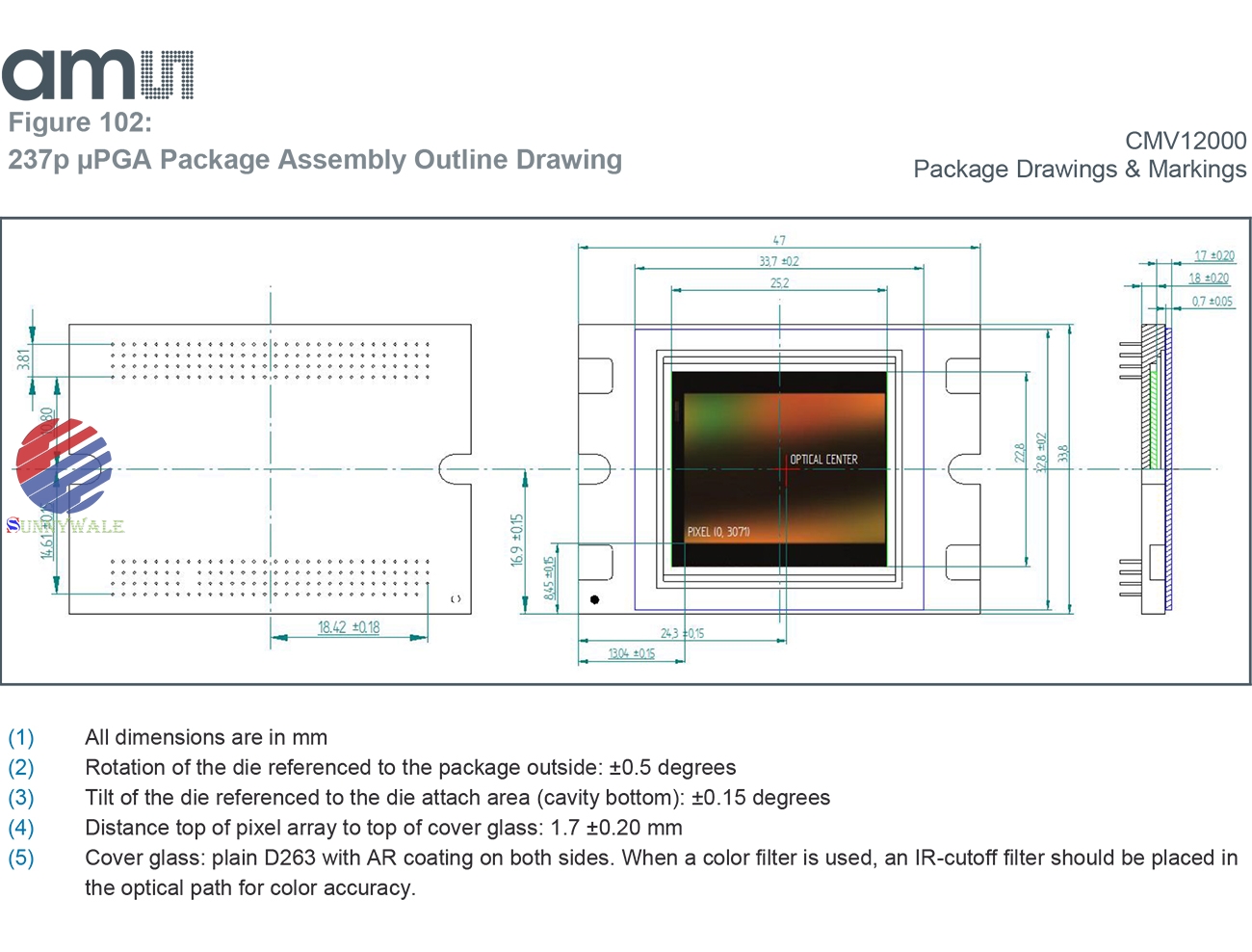
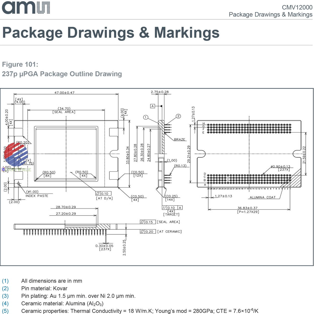
CMV12000-2E5M1PA Austria AMS OSRAM 12 megapixel (12MP) High frame rate large pixel High pixel Global shutter monochrome CMOS image sensor for industrial cameras, machine vision cameras...
CMV12000-2E5M1PA, ES12-2E5M1PA, AMS image sensor, OSRAM sensor, 12 Million Pixel (12MP) sensor, high-speed industrial camera, Machine vision, Motion capture, Global shutter, Intelligent Transportation System camera CMOS, Monochrome CMOS image sensor, high frame rate large pixel and high pixel CMOS


CMV12000-2E5M1PA General Description
The CMV12000 is a high speed CMOS image sensor with 4096 by 3072 pixels (22.5 mm x 16.9 mm) developed for machine vision and other applications. The image array consists of 5.5 μm x 5.5 μm pipelined global shutter pixels, which allow exposure during read-out. The image sensor has 64 8-, 10- or 12-bit digital LVDS outputs (serial). The image sensor also integrates a programmable gain amplifier and offset regulation. Each channel runs at 600 Mbit/s which results in 132 fps frame rate at full resolution and 12-bit. When 10-bit per pixel is used, the frame rate increases to 300 fps. Higher frame rates can be achieved in row-windowing mode or row-subsampling mode. These modes are all programmable using the SPI interface. A programmable on-board sequencer generates all internal exposure and read-out timings. External triggering and exposure programming is possible. Extended optical dynamic range can be achieved by multiple integrated high dynamic range modes.
CMV12000-2E5M1PA Key Benefits & Features
The benefits and features of CMV12000, 12Mp High Speed Machine Vision Global Shutter CMOS Image Sensor are listed below:
CMV12000-2E5M1PA Benefits
Designed for high performance applications
Capture fast moving objects
Select high frame rate or improved image quality
See bright and dark objects simultaneous
CMV12000-2E5M1PA Features
A resolution of 4096×3072 at 300 frames per second
8T global shutter pixel with true Correlated
Double Sampling (true CDS) 8-bit, 10-bit and 12-bit ADC
Standard dynamic range of 60 dB
High Dynamic Range (HDR) modes possible
CMV12000-2E5M1PA Applications
● Industrial camera
● Machine Vision
● High End Inspection
● Video/Broadcast
● Motion Capture
● Intelligent Transportation System (ITS)
CMV12000-2E5M1PA Functional Description
CMV12000-2E5M1PA Sensor Architecture
Figure 2 shows the image sensor architecture. The internal sequencer generates the necessary signals for image acquisition. The image is stored in the pixel (global shutter) and they are read out sequentially, row-by-row. On the pixel output, an analog gain is possible. The pixel values then passes to a column ADC cell, in which ADC conversion is performed. The digital signals are then read out over multiple LVDS channels. Each LVDS channel reads out 128 adjacent columns of the array. The read-out of the pixel array is performed on both sides (top and bottom) of the pixel array to speed up the read-out process and achieve the frame rate of 300 fps at full resolution and 10-bit. In each line read-out cycle, two lines are selected for read-out. In the Y-direction, rows of interest are selected through a row-decoder, which allows a flexible windowing. Control registers are foreseen for the programming of the sensor. These register parameters are uploaded via a four-wire SPI interface. A temperature sensor, which can be read out over the SPI interface, is also included.


CMV12000-2E5M1PA Pixel Array
The pixel array consists of 4096 x 3072 square global shutter pixels with a pitch of 5.5 μm (5.5 μm x 5.5 μm). This results in an optical area of 22.5 mm x 16.9 mm (28.1 mm diameter).
The pixels are designed to achieve maximum sensitivity with low noise (using CDS) and low PLS specifications. Micro lenses are placed on top of the pixels for improved fill factor and quantum efficiency.
There are 16 dark reference columns available on the sensor (columns 0 to 7 and 4088 to 4095) which can be enabled/disabled by programming the appropriate sensor register.
Analog Front End
The analog front end consists of two major parts, a column amplifier block and a column ADC block.
The column amplifier prepares the pixel signal for the column ADC and applies analog gain if desired (programmable using the SPI interface). The column ADC converts the analog pixel value to an 8-, 10- or 12-bit value and can apply a gain. A digital offset can also be applied to the output of the column ADCs. All gain and offset settings can be programmed using the SPI interface.
LVDS Block
The LVDS block converts the digital data coming from the column ADC into standard serial LVDS data running at maximum 600 Mbit/s. The sensor has 66 LVDS output pairs:
● 64 Data channels
● 1 Control channel
● 1 Clock channel
The 64 data channels are used to transfer 8-bit, 10-bit or 12-bit data words from sensor to receiver. The output clock channel transports a DDR clock (max 300 MHz), synchronous to the data on the other LVDS channels. This clock can be used at the receiving end to sample the data. The data on the control channel contains status information on the validity of the data on the data channels, among other useful sensor status information. Details on the LVDS timing and format can be found in section 7.3 of this document.
Sequencer
The on-chip sequencer will generate all required control signals to operate the sensor from only a few external control signals. This sequencer can be activated and programmed through the SPI interface.
SPI Interface
The SPI interface is used to load the sequencer registers with data. The data in these registers is used by the sequencer while driving and reading out the image sensor. Features like windowing, subsampling, gain and offset are programmed using this interface. The data in the on-chip registers can also be read back for test and debug of the surrounding system.
Temperature Sensor
A 16-bit digital temperature sensor is included in the image sensor and can be controlled by the SPI-interface. The on-chip temperature can be obtained by reading out the register with address 127.
CMV12000-2E5M1PA Operating the Sensor
This section explains how to connect and power the sensor, as well as basic recipes of how to configure the sensor in a certain operation mode.
It is recommended to decouple every physical supply pin at the sensor with a 100 nF ceramic capacitor per pin. As VDD18 and VDD_PIX draw large peak currents it is also recommended to add a larger (>10 μF) local capacitor close to the sensor for those supplies. At the voltage regulator side also enough bulk decoupling has to be foreseen.
VDD18 draws its peak current every read out line. The peak current decreases with lower data rates. Care has to be taken in the supply and decoupling design so that VDD18 is always above 1.93 V during these peaks (so max. 50 mV dip) to guarantee sensor performance. The voltage regulator should be able to handle the 1.7 A.
VDD_PIX draws a short but large peak current during FOT. Care has to be taken in the supply and decoupling design so that VDD_PIX is always above 2.9 V during these peaks (so max. 100 mV dip) to guarantee sensor performance. The peak current should be handled by the decoupling capacitors, not the voltage regulator.
For VDD33 and VDD_RES the peak currents are lower, but still care has to be taken not allowing the voltages dips outside the voltage range.
The voltage required is the voltage on the supplies to guarantee the best sensor performance. The voltage range is the range the voltage should stay within (so during current peaks) to guarantee sensor performance. If the supply is outside the voltage range, the sensor might still be functional but performance is not guaranteed. The voltage absolute maximum is the range outside which (permanent) sensor malfunction might occur.
For more details on the power figures and peak plots, an application note is available. This supply needs therefor decent decoupling to dampen the current peak.
The sensor will heat up above ambient (+ ~20/40 °C idle/running at 600 MHz). Therefore decent system heat management is needed to keep the sensor junction temperature below the specifications limit of 70 °C.
Biasing
For optimal performance, some bias pins need to be decoupled to ground or to VDD. Please refer to the pin list for a detailed description for every pin and the appropriate decoupling.
......
All of the above pictures are taken after matting the online showing, what you see is what you get.
Click or copy the link to free download the datasheet PDF file.
Freight is free when you buy 2 pieces in China, if you have CMV12000 inventory, you can sell to me, if you need buy CMV12-2E5M1PA, you can ask me to buy.
If you want to know about similar products CMV2000,
CMV4000, or click here,or Visit The official website:
sunnywale.com,Search the keywods“
CMV”,it can show more details.
For more details and HD images, please copy the following link to open in your browser to view our official website;or visit our official website:
Sunnywale.com , searching keyword "CMV12000".
For more details, please click
中文版
