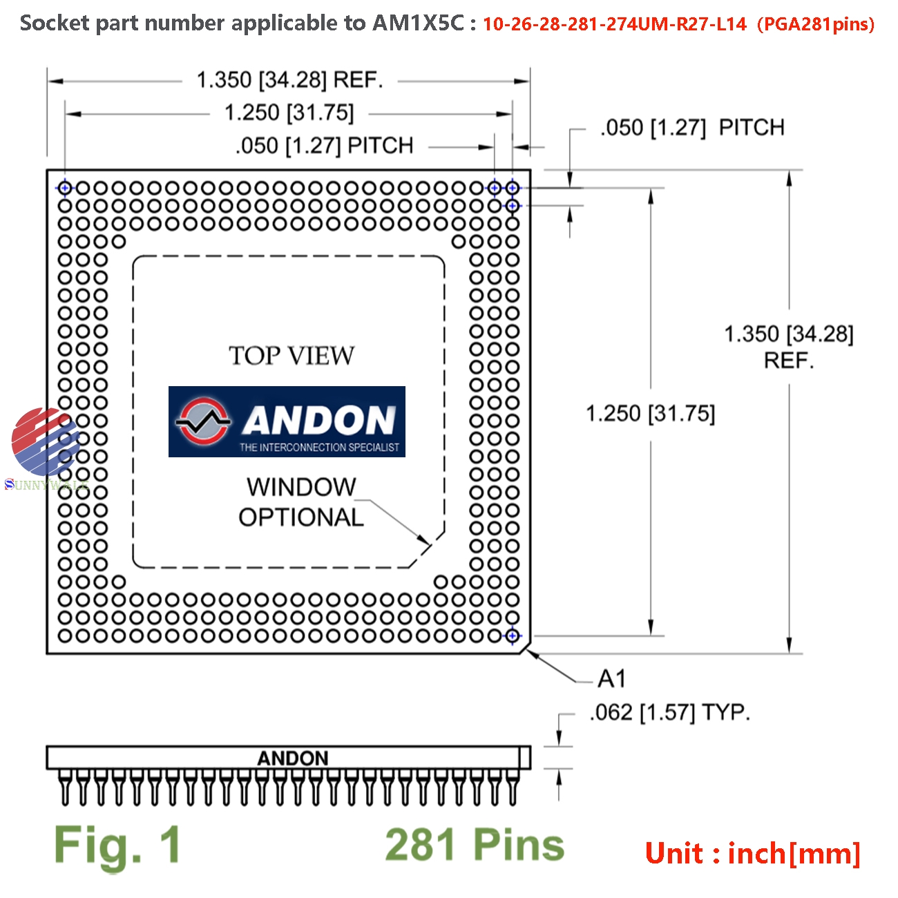
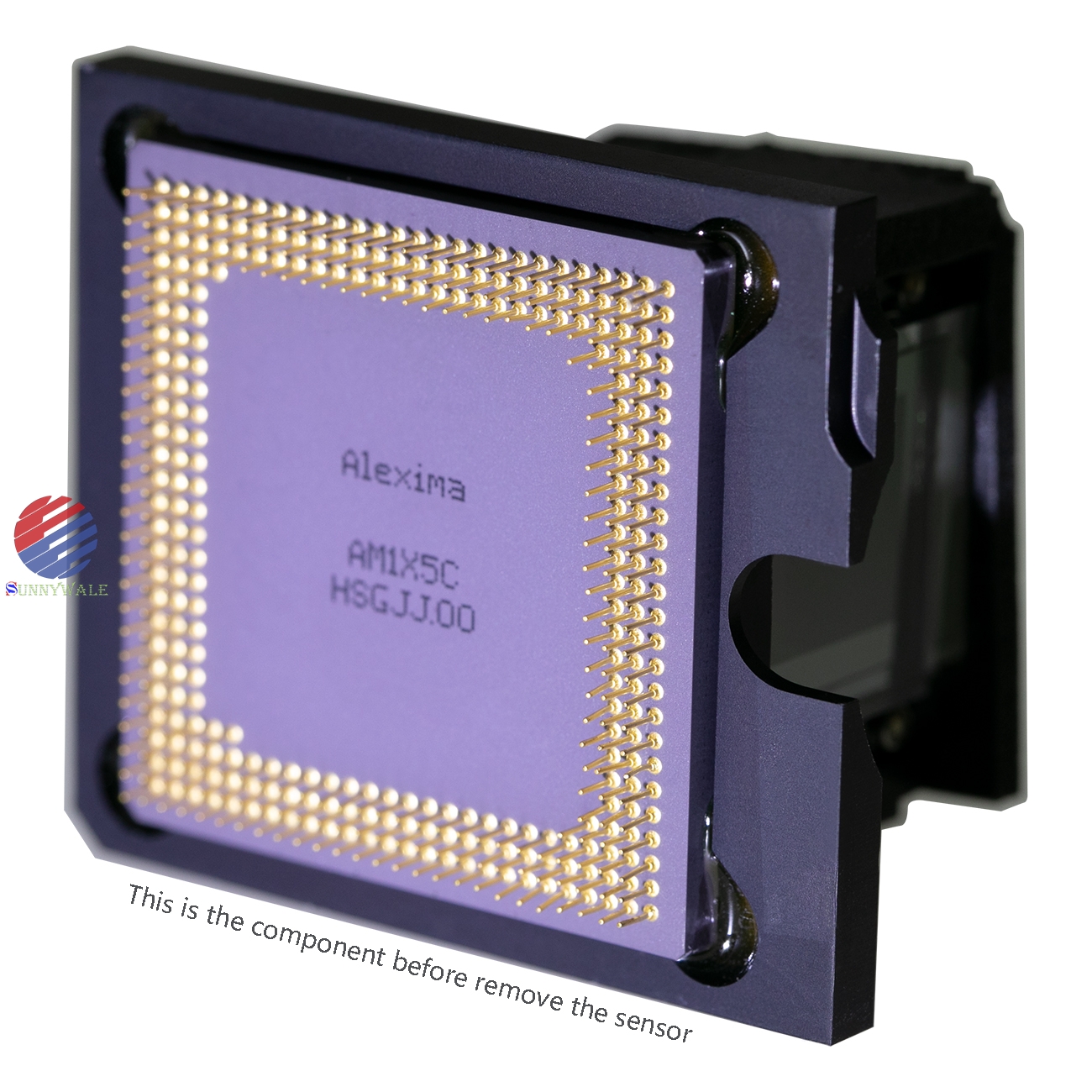
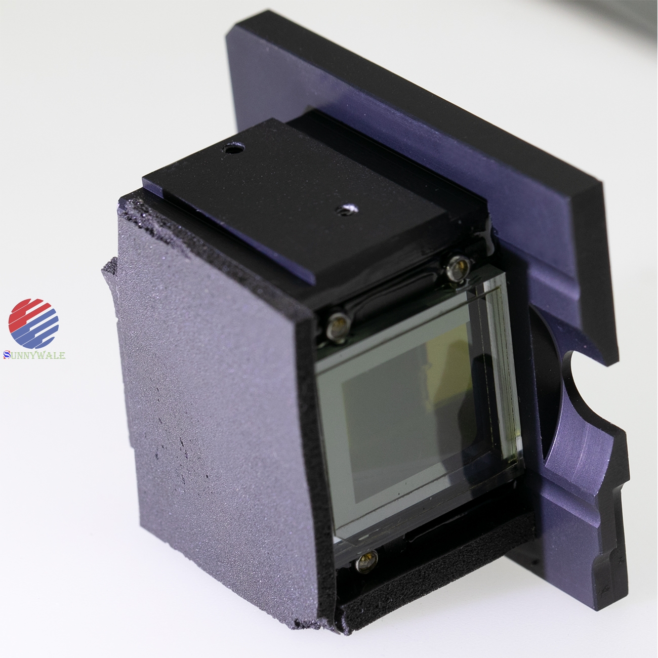
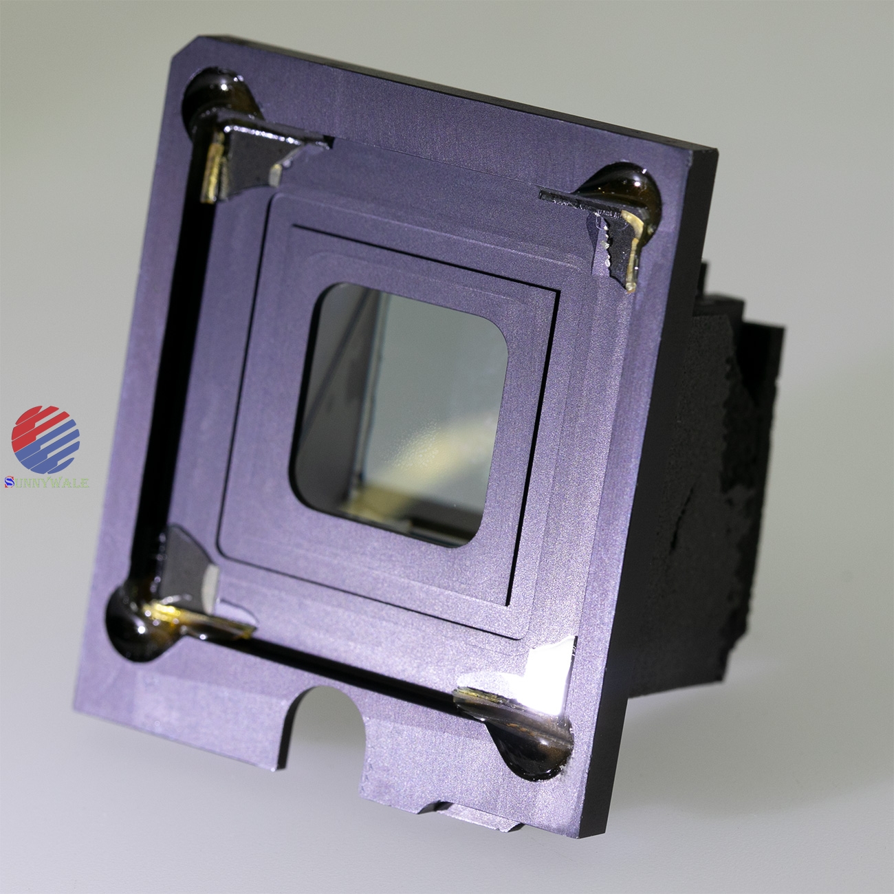
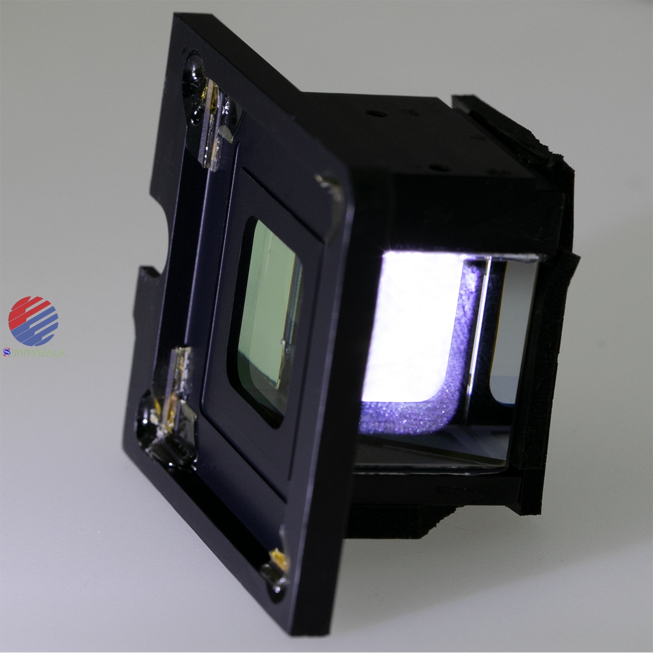
AM1X5C Alexima (LUXIMA) megapixel 1024x1024PX@5000fps 13.9μmx13.9μm pixel Global Shutter Exposure Science Experiment Ultra High speed camera CMOS image sensor
2023-04-02 16:40:05
Buy Now
AM1X5C, Alexima, LUXIMA, megapixel, 1024x1024PX, 5000fps, 13.9μmx13.9μm pixel, global shutter exposure, ultra high speed camera for scientific experiment, CMOS image sensor,IDT Y4 camera cmos image sensor,oSTreaming 15220-0100 sensor,Legacy-mm-final
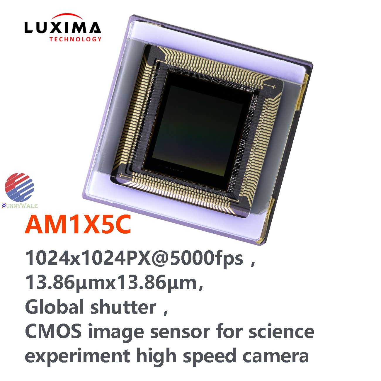
AM1X5C is a 1K*1K (1024x1024)pixel CMOS sensor with a pixel size of 13.86μm and a full resolution of 5000fps Global shutter.
New or used are available, the old spot is not limited to purchase, any quantity can be bought, the new minimum order of 100 pieces -2-3 weeks delivery.
 INTRODUCTION
 AM1X5 is a super high speed digital CMOS sensor. This sensor targets frame rate from 3,000fps minimum to 5,000fps maximum, with the data throughput of 3-5 Gpix/s. This is 2.5-4 times faster than the throughput of 1.3 Gpix/s from the previous generation MV03 sensor. An increase in data rate is achieved through using 4 ADCs per column, wider (8 pairs) width of the data register bus, and employing double data rate SSTL-2 I/O pads. Another feature of AM1X5 is a buried channel shutter pixel. We expect a breakthrough in sensitivity from the pixel.
The sensor has two column readout blocks (on top and in the bottom) which include amplifier circuits, ADCs utilizing SAR (successive-approximation) method, and Register block where the ADC data is temporarily stored for readout. The readout from the SAR registers as well as the sensor controls are arranged as a 4 quadrant readout & control architecture, which allows local
control over SAR ADCs and local data readout, both essential for high speed operation of the sensor. The sensor also has some biases and all current sources generated internally. Although, many critical voltages to this chip are required to be generated externally.
2.0 PIXEL ARRAY
There are total of 1028x1026 pixels including 1014x1024 active pixels, 2 dark row and 14 dark column readable pixels, 7 on each side. Other boundary pixels are not readable and serve only for reducing of an edge effect in the response uniformity of the active pixels. A drawing of the pixel array is sketched in datasheet's Fig.2.
7.0 SENSOR CONTROLS
7.1. Overview
There are four sensor control blocks in the four corners of the chip. The two upper control blocks serve the upper readout, the two bottom control blocks serve the bottom readout. The upper internal controls are somewhat autonomous from the bottom controls. Small timing misalignment between the top and the bottom internal control pulses shall not cause any conflict of drivers. But, there shall be good symmetry of operation between the left and the right controllers, because they are driving the pixel array and column ADCs from both sides. To facilitate this symmetry, the chip master clock is split into the clk_top and clk_bot serving the top and the bottom of the chip, respectively. Also, the clock pads are placed in the middle of the pad ring (at the top, and bottom) to built a clock tree which is left-right symmetrical.
To reduce the power consumption and increase reliability of controls, the internal controls are generated from the Clock divided by two. To synchronize the divided clock with external controls, an access to the divider reset is provided. Pin DIV_RB serves as an asynchronous reset bar control over two frequency dividers. A short 1-2 clock LOW pulse once a row or once a frame is OK to synchronize the counter.
Row driver is placed on one both sides of the chip, but the global shutter controls PD_n, PD2_n, and TX_n are on one side of the chip. To insure these controls come to the row drivers simultaneously, they are registered. However, if the setup time for these controls is too short, the ontrols after registering may get split by 1 clock cycle. This may cause some shutter artifacts, so we need to set up the setup time requirement.
Row addressing controls are also registered. For similar reason, they also need a proper setup
time.
There are four important controls start_row/read which trigger row operations and readout operations. These pads are on one side of the chip, so the signal propagation time to the left and the right controllers is different. The difference can reach ~ 4 ns. This dictates a long setup time for these two pulses to exclude the situation when the left controller senses the “Start” command one clock earlier than the right controller, which may cause a chip malfunction.
The hold time > 0ns is needed because the clock signal delay may appear to be longer compared to the control delay. The clock signal experiences multi-stage buffering because of the clock tree structure made for this signal. If, for instance, the clock and a control signal are generated in the same FPGA, and the control signal is a derivative of the clock .
Product applications:
animation industry,
trajectory shooting,
process control shooting,
car collision shooting,
PCB board detection,
LCD detection,
high-speed radio/sports TV,
dental camera,
traffic control
high-speed applications.
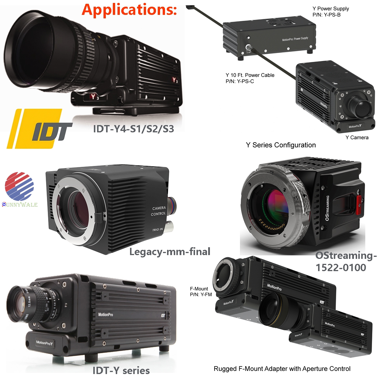
Alexima's latest image sensor, the Am1X5, aims for higher frame rates. The device features a 1k x 1k (1024x1024)pixel, a 5,000frame/s digital CMOS sensor and a global shutter, and was recently integrated into Y4, a high-speed camera from IDT capable of running at a 1016 by 1016 pixel resolution at 3,000 frames per second


 AM1X5C applications for high speed camera cases:
 A brief introduction to LUXIMA Technology
Luxima Technology, Inc. is based in Pasadena, California, USA, and was founded by Dr. Alexander Krymski and Dr. Lin Ping Ang. The company's founders are CMOS image sensor design experts with more than 60 years of experience in the image sensor industry. They hold about 50 patents in the area of image sensors.
The founder worked at Photobit, where he helped invent innovative design techniques that are still used today in many CMOS image sensors. They have extensive design knowledge in the image sensor architecture of ultrafast high resolution global shutter image sensors and the low noise readout architecture of high performance DSC image quality image sensors.
Luxima Technology was founded to create best-in-class custom CMOS imaging solutions for the high-speed image sensor market. In emerging markets, innovative design techniques are critical to addressing application needs.
Luxima Technology also has a strong focus on custom design, paying close attention to every step of the design phase, from design specifications to mid-term design reviews to device characterization. Luxima Technology's experience enables us to deliver products in a short period of time through close collaboration with our customers.
All of the above pictures are taken after matting the online showing, what you see is what you get.
Click or copy the link to free download the AM1X5C datasheet PDF file.
Freight is free when you buy 2 pieces in China, if you have AM1X5C inventory, you can sell to me, if you need buy AM1X5C, you can ask me to buy.
If you want to know about similar products ***, or click here,or Visit The official website:
sunnywale.com,Search the keywods“**”,it can show more details.
For more details and HD images, please copy the following link to open in your browser to view our official website;or visit our official website:
Sunnywale.com , searching keyword "AM1X5C".
If you want to read the introduction in English, please Clict the
中文版
