IMX490, SONY 1/1.55 backlit starlight night vision image sensor, high dynamic HDR automotive assistance driving collision prevention, obstacle avoidance sensor, traffic light sign recognition, advance
It sells ICs on modules, not modules on pictures!
IMX490, SONY 1/1.55 backlit starlight night vision image sensor, high dynamic HDR automotive assistance driving collision prevention, obstacle avoidance sensor, traffic light sign recognition, advanced iteration of IMX390
IMX490, SONY 1/1.55 backlit image SENSOR, starlight CMOS, ultra-low illumination, moonlight level visibility, automotive imaging industry's highest pixel image creator, HDR CMOS SENSOR, 120db high dynamic, SONY car gauge sensor new, 5.4MP cmos, 120db HDR imaging, LED flicker mitigation function, identification of obstacles and traffic lights, identification of traffic signs, instead of IMX390 advanced products, night vision CMOS chip, automotive assistance driving anti-collision, obstacle avoidance sensor
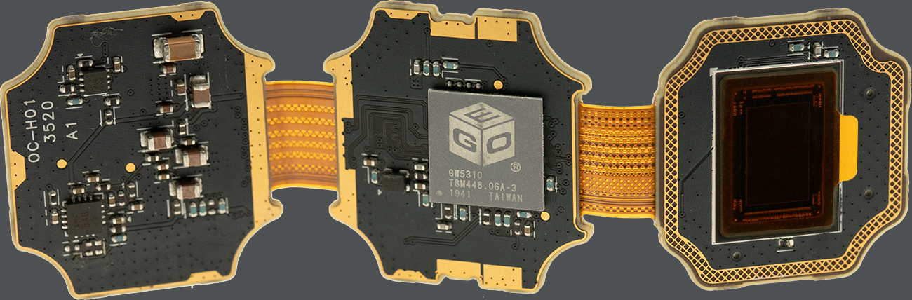
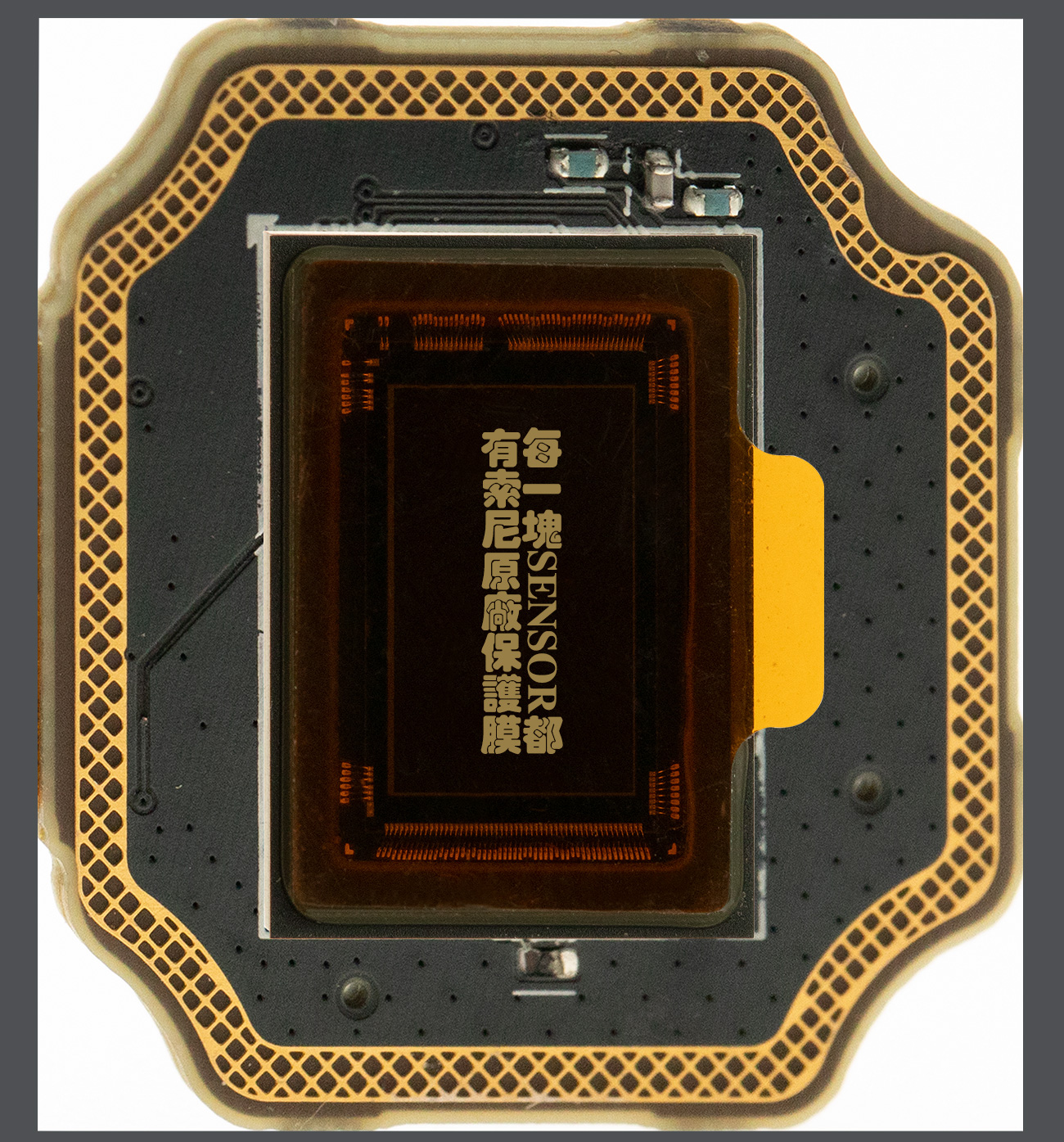
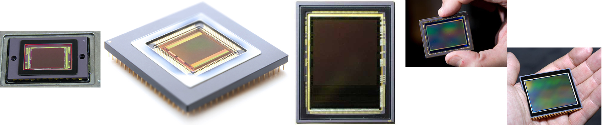
IMX490 SONY 1/1.55-inch 5.44 Mega pixels CMOS image sensor for automotive
IMX490 SONY 1/1.55-inch 5.44 Mega pixels CMOS image sensor for automotive
1. The IMX490 back-illuminated stacked CMOS Product Features image sensor achieves simultaneous HDR shooting and LED flicker(*1) mitigation and features industry's highest(*2) 5.4
effective megapixels,(*3) enabling wide-angle shooting for ADAS/autonomous driving.
2. 120dB(*4) HDR function three times that of conventional product, plus motion artifact mitigation(*5).
3. High sensitivity of 2280 mV (standard value: F5.6) improved by approximately 15% over that of conventional product.
*1: LED flickering that occurs when photographing LED indicators, traffic lights, etc.
*2: As of announcement on December 18, 2018
*3: Based on image sensor effective pixel specification method
*4: In accordance to the EMVA 1288 standard. 140dB when set to prioritize dynamic range.
*5: Depends on conditions. A function introduced with the IMX390 (current model).
*6: Conforms to ASIL-D. A portion of the failure rate metric has been tailored.
Product Features
. 1/1.55-type back-illuminated stacked CMOS image sensor
. Unit cell size: 3.0μm
. Number of recommended recording pixels: 2896 (H) X 1876 (V) approx. 5.40M pixels
. Maximum frame rate in full pixel reading: AD10bit 40fps, AD12bit 30fps
. High dynamic range (HDR) function with 120dB (EMVA 1288 standard, 140dB when set to prioritize dynamic range.)
. LED flicker mitigation function
. Variable speed shutter function
. MIPI CSI-2 serial output (4 lane / 2 lane)
. Temperature sensor
. Support security feature for automotive
. ISO 26262/ASIL-D*6
. AEC-Q100 Grade 2
Product Specifications
. Model name:IMX490
. Number of effective pixels:2896 (H) x 1876 (V) 5.40 megapixels
. Image size:Diagonal 10.36 mm (Type 1/1.55)
. Unit cell size:3.0 μm (H) X 3.0 μm (V)
. Frame rate:Full pixel reading:AD10bit 40fps, AD12bit 30fps
. Sensitivity (F5.6 Standard Value, 1/30 sec. exposure time):2280mV (Green pixel)
. Dynamic range (EMVA Standard 1288):120dB (140dB when prioritizing dynamic range)
. Power supply:
Analog:3.3V
Digital:1.1V
Interface:1.8V
. Interface: MIPI CSI-2 serial output (4 lane / 2 lane)
. Package :124pin Plastic BGA
. Package size: 15.35 mm X 11.68 mm
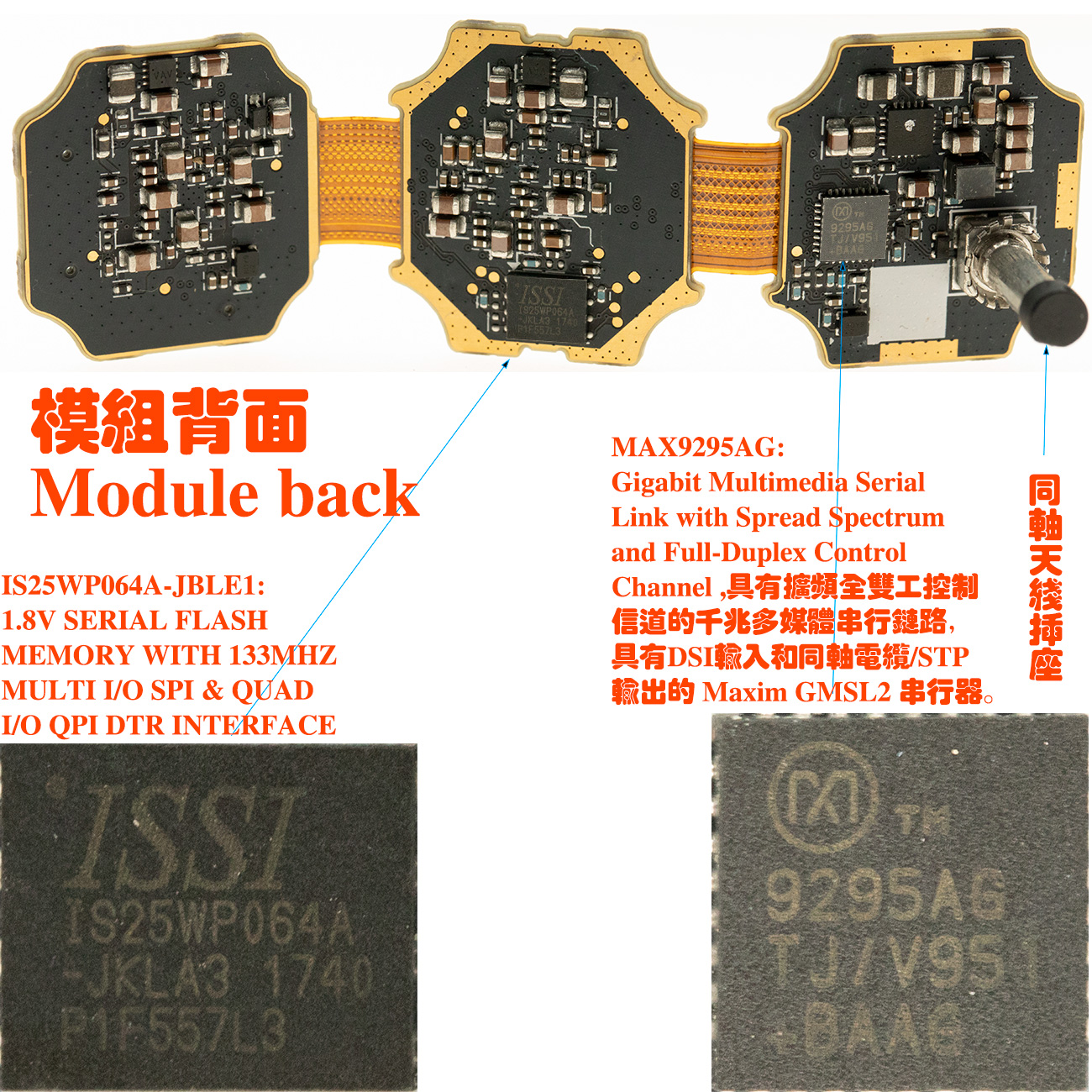
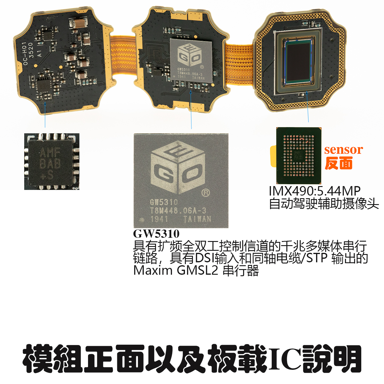
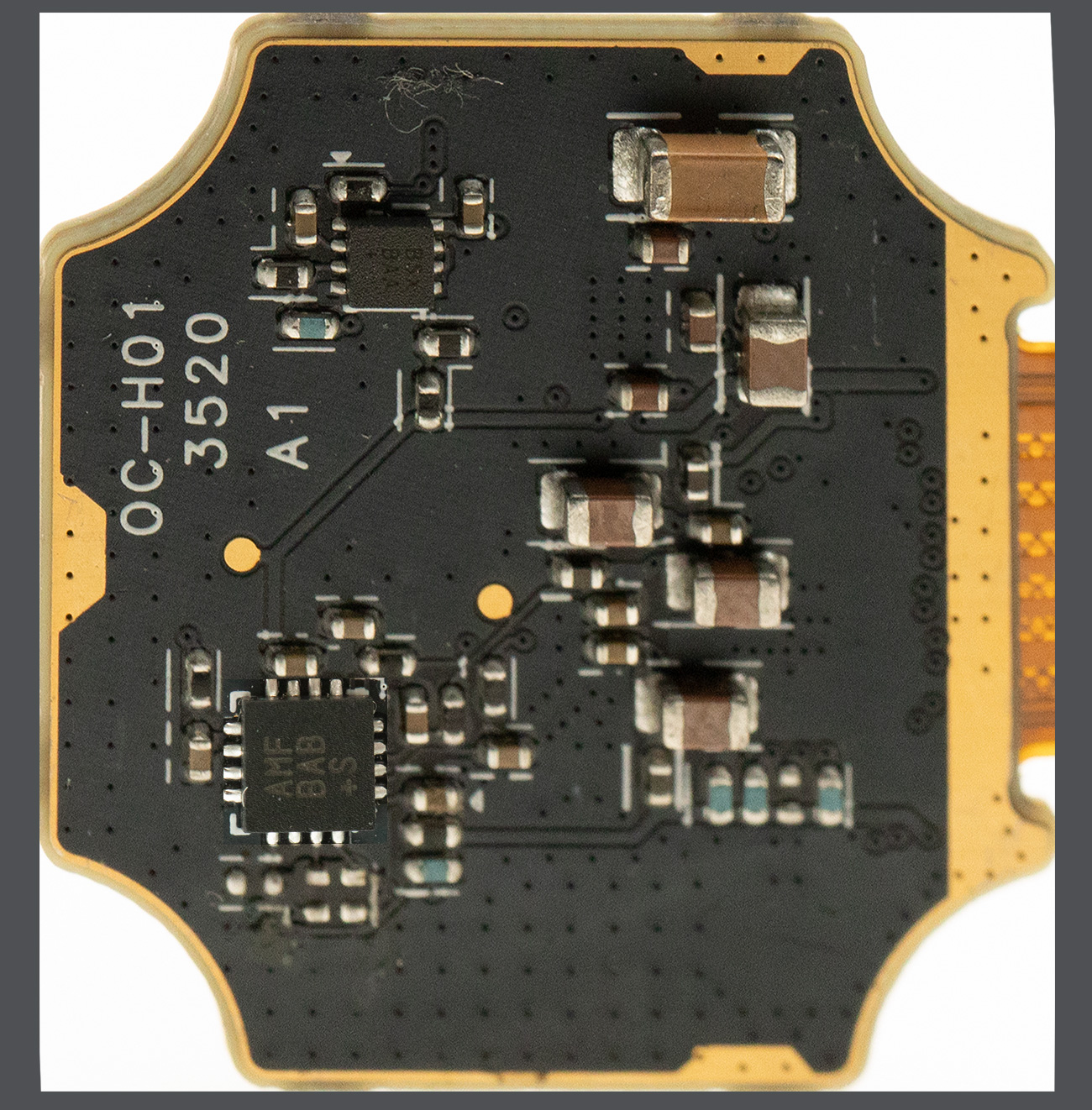
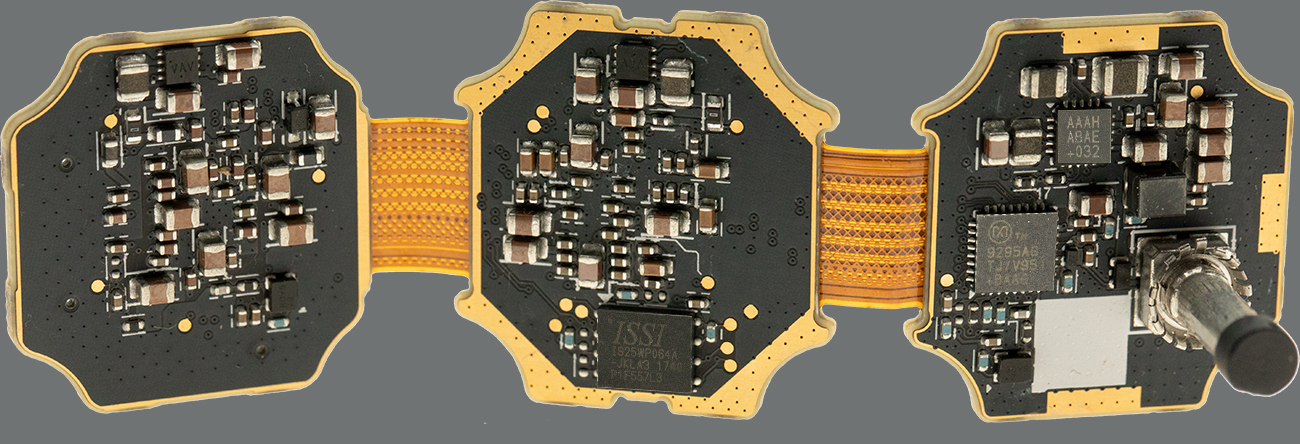
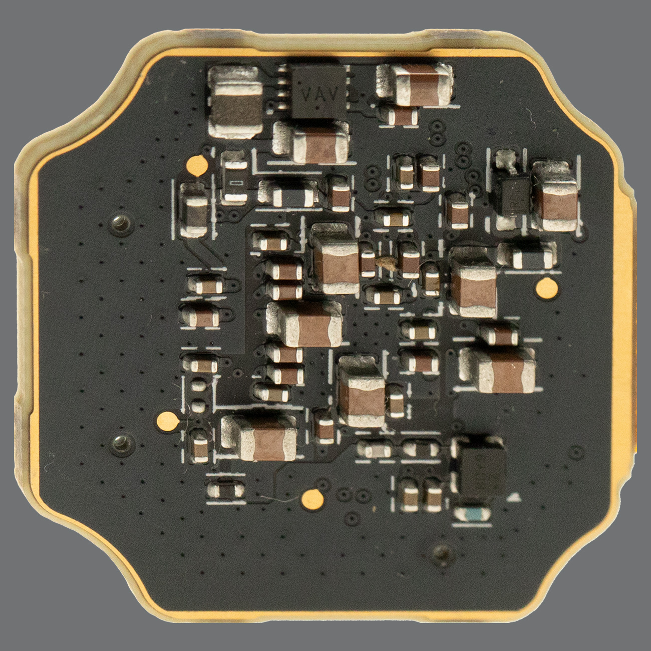
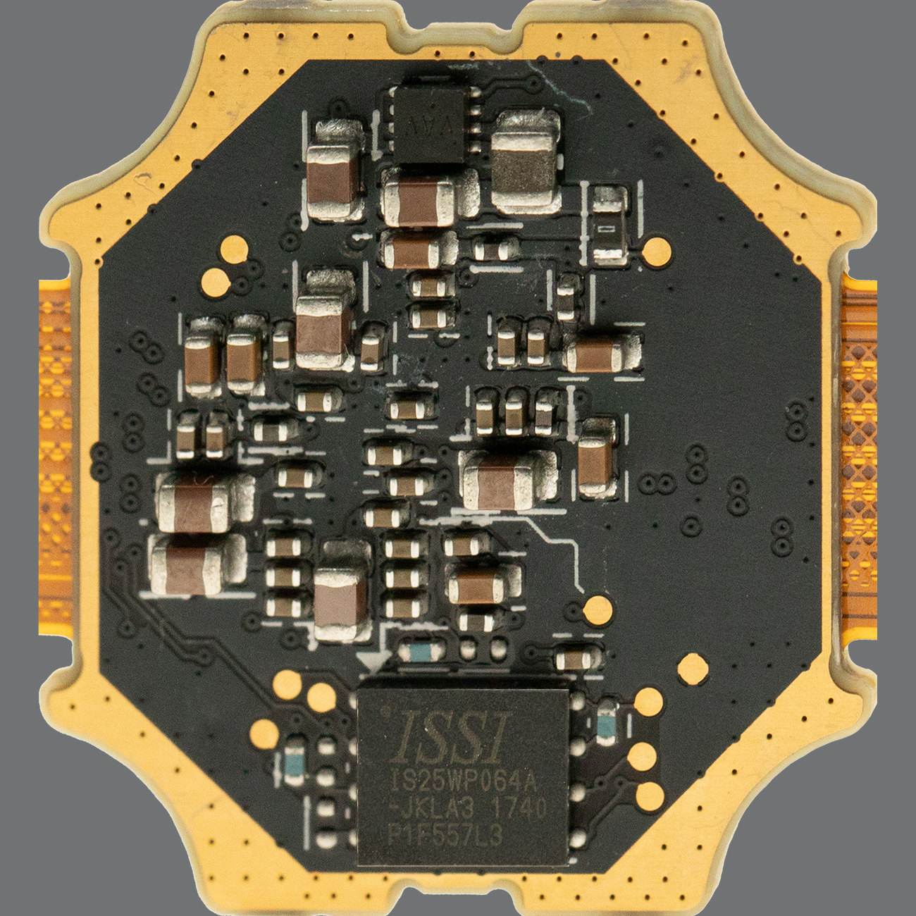
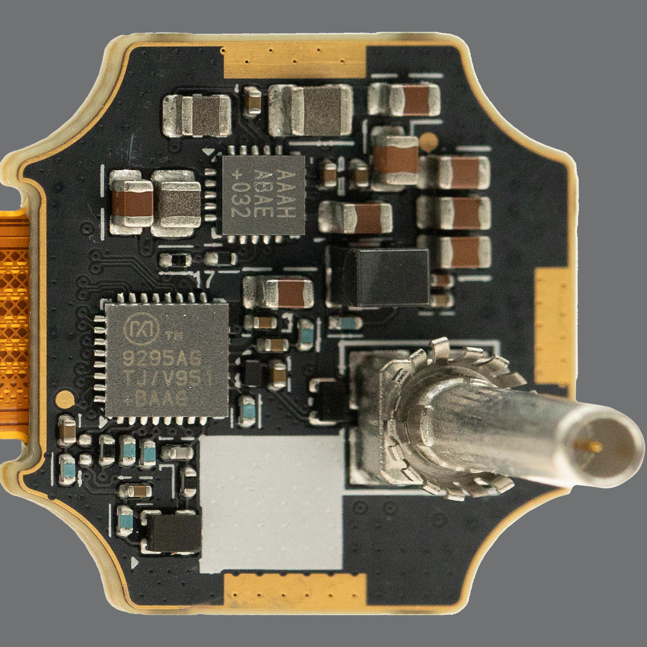
IMX490周边板载IC介绍:
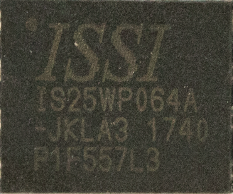
IS25WP064A-JKLA3:1.8V SERIAL FLASH MEMORY WITH 133MHZ MULTI I/O SPI & QUAD I/O QPI DTR INTERFACE
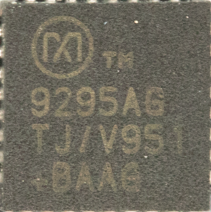
MAX9295AG:Gigabit Multimedia Serial Link with Spread Spectrum and Full-Duplex Control Channel ,
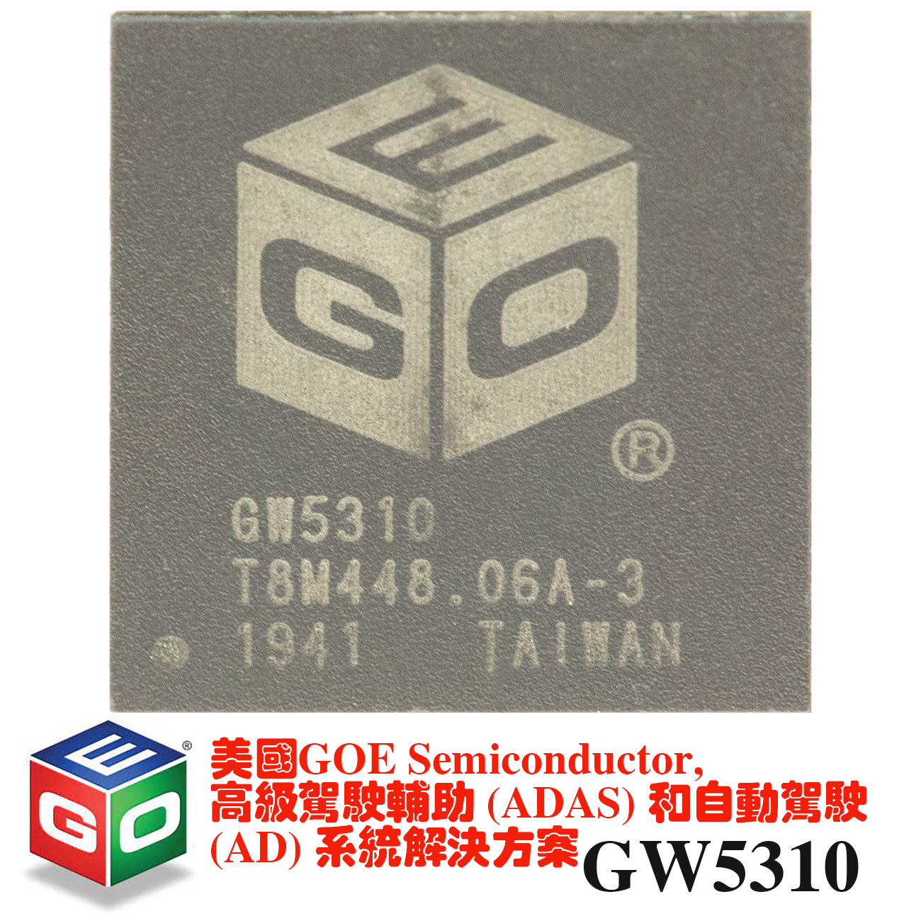
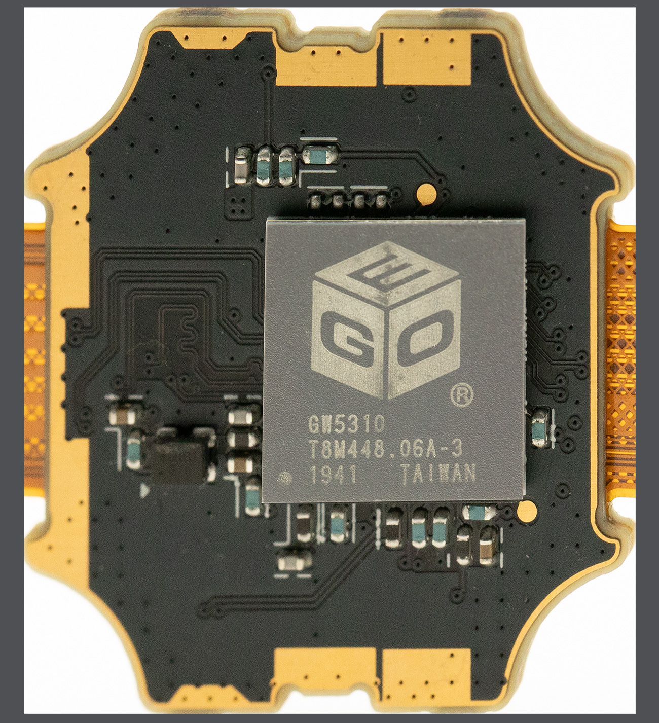
GW5300(GW5310)
GENERAL DESCRIPTION
The GW5300 is an advanced Camera Video Processor (CVP) System-on-Chip (SoC) designed for high-resolution sensor automotive applications. The GW5300 includes GEO’s proprietary 5th-generation eWARP? geometric processor, innovative High Dynamic Range (HDR) Image Signal processor (ISP), and 2D graphics functionality. Designed in a 28nm process to enable small, low power automotive cameras on-the-edge, the GW5300 supports ASIL B and AEC Q100 Grade 2.
The HDR ISP supports up to 8MP30 or 5MP60, and LED Flicker Mitigation (LFM) techniques by pairing with the latest automotive sensors from On Semi, Sony, Omnivision, Samsung, Panasonic, and ST. GW5300’s on-chip combining of up to four exposures drives dynamic range up to 145dB. The 2D Vector Graphics Engine renders high resolution real-time graphics to overlay on the video stream enabling compelling user interfaces.
The GW5300 reduces system component count by requiring no external DDR memory and incorporating dual camera inputs. GW5300 based designs can be rapidly brought to market by leveraging GEO’s SDK and EVK.
GW5300 BLOCK DIAGRAM
GW5200 Block Diagram
APPLICATIONS
. ADAS/AD Cameras
. Augmented Reality
. Videoconferencing
. DVR
FEATURES
eWARP? Geometric Processor
. 5th-gen eWARP? geometric processor
. Ultra-wide field of view (FOV) lens distortion correction
. Dynamic Electronic Pan/Tilt/Zoom (ePTZ)
. AutoCAL? digital calibration for extrinsic camera alignment
. Ultra-low latency (typically 1/6th of a frame)
HDR Image Signal Processor
. Supports up to 8MP30, 5MP60, or 12MP20 image sensors
. High Dynamic Range (HDR) processing
. Advanced spatial (2D) noise reduction
. Zone-based statistics for AE and AWB
. Dynamic defect and lens shading correction
. Color Noise Reduction, Purple Fringe Correction
. Defog support
Overlay Graphics
. Blending of up to 8 layers
. Fully independent alpha values across layers and pixels
. Vector Graphics Engine
On-the-fly rendering: 1920×1080 at 60fps
High quality multi-sampled anti-aliased rendering
. Pre-rendered bitmaps
Up to 4096×4096 bitmap resolution
256 colors selectable from 24bpp true color range per layer
In-line on-chip de-compression for memory savings
System Features
. CAN 2.0B, CAN FD, 3x I2C, 2x SPI, 2x UART, 15x GPIO, 3x PWM, JTAG, eFuse
I/O Interfaces
. Input: 2x MIPI CSI-2 4-lane @ 1.5Gbps/lane
. Output: 1x or 2x MIPI CSI-2 4-lane @1.5Gbps/lane
. Input: 16-bit parallel @ 150MHz
. Output: 16-bit parallel @ 150MHz
. Note: Parallel input and output not supported together
Automotive Safety
. ISO26262 Safety Element out of Context (SEooC) – ASIL B
. System health monitoring, status reporting, and Safe State
. ECC support for all processor code spaces
. Interface support for error detection and correction modes
. Embedded video and system statistics in output stream
. Voltage and temperature sensors, watch dog timer
Electrical Specifications
. Supply voltages:
Core: 0.9V ±5%
PLL and MIPI: 1.8V ±5%
I/O: 1.8V or 2.5V or 3.3V ±5%
. Power:
. Automotive: AEC Q100 Grade 2 (-40°C to 105°C)
. Industrial: -40°C to 85°C
Package
. 169-ball TFBGA 7mm x 7mm, 0.50mm pitch (GW5300 – 1x MIPI output)
. 196-ball TFBGA 10mm x 10mm, 0.65mm pitch (GW5310 – 2x MIPI output)
. RoHS/Lead-Free
GEO SEMI ANNOUNCES HIGH RESOLUTION ADAS AND AUTONOMOUS DRIVING SYSTEMS DESIGN WINS
GEO Semi Announces High Resolution ADAS and Autonomous Driving Systems Design Wins
The GW53x0 Product Provides High Resolution Solutions for Future ADAS and AD Automotive Systems
SAN JOSE, Calif. , July 28, 2020 GEO Semiconductor Inc. (“GEO”), the market leader in camera video processors (CVP) for automotive cameras, today announced new design wins for Autonomous and ADAS system applications using the GW53x0 product and supporting high resolution and HDR processing.
GEO’s application specific camera video processors include both the GW4 and GW5 product lines. These products feature world class high dynamic range image processing, geometric processing, featuring GEO’s eWARP? technology, overlay graphics, and in the case of the GW54x0, a DSP processor for computer vision processing.
Leveraging a versatile design architecture with a small package footprint, low power design, and low cost, without requiring an external DRAM memory, the GW4 and GW5 products stand out as a solution to a number of camera and video applications in the fast developing automotive market.
Today, GEO is engaged with multiple OEMs and industry processor partners for Advanced Driver Assistance (ADAS) and Autonomous Driving (AD) system solutions. For these applications GEO’s GW53x0 product supports high resolution (8 megapixel), high dynamic range automotive image sensors with unique Color Filter Array patterns such as RGGB, RCCB, and RYYCy. The GW53x0 enables customers to customize the image quality to support viewing outputs as well as optimizing the tuning to feed today’s Computer Vision processors for decision making in ADAS or AD applications.
“The GW53x0s high resolution HDR capability, ASIL B support, and the eWARP? processors ability to correct distortion and provide Region of Interest (ROI) selection make it an ideal processor for many ADAS applications,” said John Casey, GEO VP and GM for Automotive. “With design wins at traditional OEM’s, many of the emerging AD system and ride sharing companies, as well as solutions with multiple Autonomous Driving chip suppliers, GEO is well positioned to participate in the next generation ADAS and AD automotive application space.”
The GW53x0 is in Mass Production, supports up to 12 megapixel resolution, full HDR processing, and is capable of processing RGGB, RCCB, and RYYCy color filter sensor designs. The product supports integration into ASIL B systems, and simultaneously outputs a YUV color processed video stream while providing a RAW video stream over CSI-2 MIPI outputs. The GW5300 is available in 7mm x 7mm BGA package with 0.50mm ball pitch and the GW5310 is available in 10mm x 10mm BGA package with 0.65mm ball pitch.
About GEO Semiconductor
GEO Semiconductor Inc. is a private fabless semiconductor company developing camera video processors for automotive viewing and ADAS cameras. GEO’s value proposition is to provide automotive Tier-1s with the best products, tools, and support to guarantee exceptional image quality and system performance. GEO is headquarteredin San Jose, CA with global representation in the U.S., Canada, Europe, China, Japan, Korea, and Taiwan. The company is led by world-class imaging and video professionals with extensive experience in research, implementation, and optimization of image signal processing, geometric processing, and computer vision processing for embedded platforms.
https://en.sunnywale.com/uploadfile/2022/0313/IMX490车规简介Awin.pdf
,Click or copy the link to free download the datasheet PDF file.
Freight is free when you buy 2 pieces in China, if you have IMX490 inventory, you can sell to me, if you need buy IMX490, you can ask me to buy.
If you want to know about similar products IMX390, IMX459, or click here,or Visit The official website: sunnywale.com,Search the keywods“IMX390,IMX459”,it can show more details.
For more details and HD images, please copy the following link to open in your browser to view our official website;or visit our official website: Sunnywale.com , searching keyword "IMX490".
If you want to read the introduction in English, please Clict the 中文版
Buy now IMX490