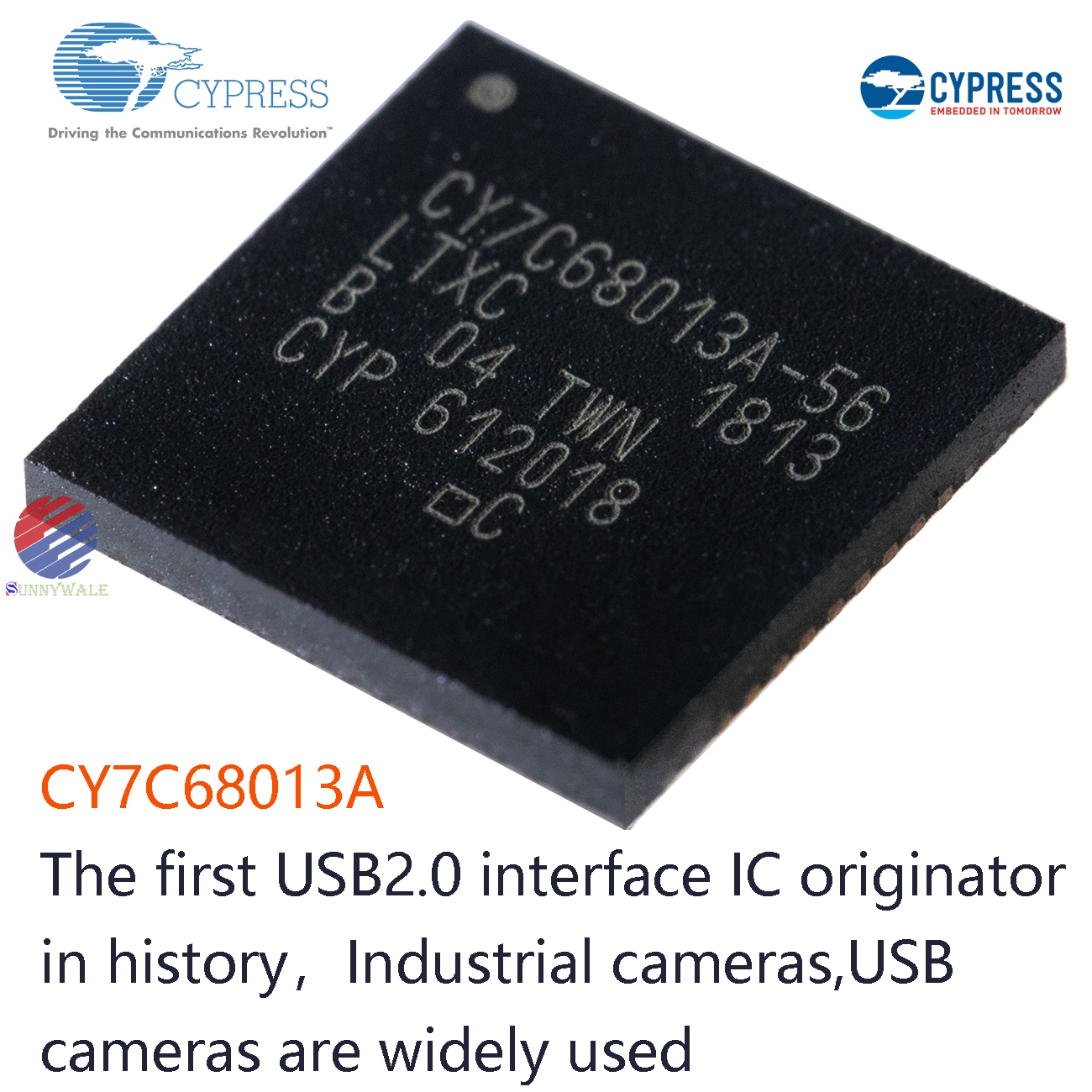
CY7C68013A-56LTXC Cypress EZ-USB FX2 USB2.0 interface IC, USB camera industrial camera microcontroller
2023-05-23 18:13:38
Buy Now
CY7C68013, Cypress, EZ-USB FX2, USB2.0 interface IC, USB camera IC, industrial camera USB microcontroller
1.0 EZ-USB FX2(TM) Features
● Single-chip integrated USB 2.0 Transceiver, SIE, and Enhanced 8051 Microprocessor
● Software: 8051 code runs from:
— Internal RAM, which is downloaded via USB
— Internal RAM, which is loaded from EEPROM
— External memory device (128 pin package
● Four programmable BULK/INTERRUPT/ ISOCHRONOUS endpoints
— Buffering options: double, triple and quad
● 8- or 16-bit external data interface
● GPIF
— Allows direct connection to most parallel interface — Programmable waveform descriptors and configu-ration registers to define waveforms
— Supports multiple Ready (RDY) inputs and Control
(CTL) outputs
● Integrated, industry standard enhanced 8051:
— Up to 48-MHz clock rate
— Four clocks per instruction cycle
— Two USARTS
— Three counter/timers
— Expanded interrupt system
— Two data pointers
● Supports bus-powered applications by using renumer-ation
● 3.3V operation
● Smart Serial Interface Engine
● Vectored USB interrupts
● Separate data buffers for the SETUP and DATA portions of a CONTROL transfer
● Integrated I2C-compatible controller, runs at 100 or 400 kHz
● 48-MHz, 24-MHz, or 12-MHz 8051 operation
● Four integrated FIFOs
— Brings glue and FIFOs inside for lower system cost
— Automatic conversion to and from 16-bit buses
— Master or slave operation
— FIFOs can use externally supplied clock or asyn- chronous strobes
— Easy interface to ASIC and DSP ICs
● Special autovectors for FIFO and GPIF interrupts
● Up to 40 general-purpose I/Os
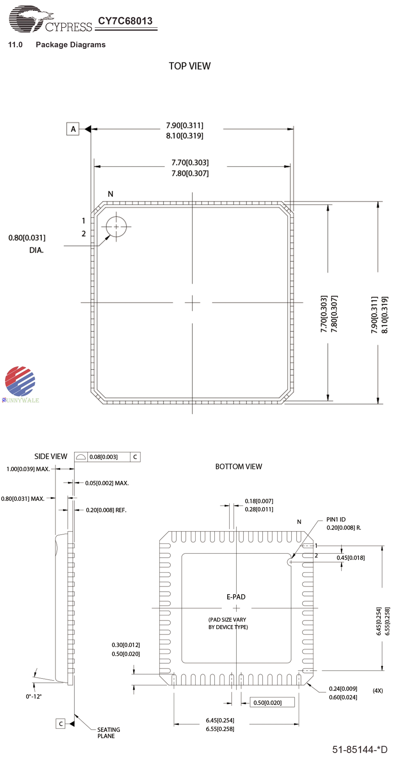
● Four package options—128-pin TQFP, 100-pin TQFP, 56-pin QFN and 56-pin SSOP
● Four packages are defined for the family: 56 SSOP, 56 QFN, 100 TQFP, and 128 TQFP
Cypress’s EZ-USB FX2? is the world’s first USB 2.0 integrated microcontroller. By integrating the USB 2.0 trans-ceiver, SIE, enhanced 8051 microcontroller, and a program-mable peripheral interface in a single chip, Cypress has created a very cost-effective solution that provides superior time-to-market advantages. The ingenious architecture of FX2 results in data transfer rates of 56 Mbytes per second, the maximum allowable USB 2.0 bandwidth, while still using a low-cost 8051 microcontroller in a package as small as a 56 SSOP. Because it incorporates the USB 2.0 transceiver, the FX2 is more economical, providing a smaller footprint solution than USB 2.0 SIE or external transceiver implementations. With EZ-USB FX2, the Cypress Smart SIE handles most of the USB 1.1 and 2.0 protocol in hardware, freeing the embedded micro-controller for application-specific functions and decreasing development time to ensure USB compatibility. The General Programmable Interface (GPIF) and Master/Slave Endpoint FIFO (8- or 16-bit data bus) provides an easy and glueless interface to popular interfaces such as ATA, UTOPIA, EPP, PCMCIA, and most DSP/processors.
2.0 Applications
● DSL modems
● ATA interface
● Memory card readers
● Legacy conversion devices
● Cameras
● Scanners
● Home PNA
● Wireless LAN
● MP3 players
● Networking.
The “Reference Designs” section of the cypress website provides additional tools for typical USB 2.0 applications. Each reference design comes complete with firmware source and object code, schematics, and documentation. Please visit http://www.sunnuwale.com for more information.
3.0 Functional Overview
3.1 USB Signaling Speed
FX2 operates at two of the three rates defined in the Universal Serial Bus Specification Revision 2.0, dated April 27, 2000:
● Full speed, with a signaling bit rate of 12 Mbps
● High speed, with a signaling bit rate of 480 Mbps
3.2 8051 Microprocessor
The 8051 microprocessor embedded in the FX2 family has 256 bytes of register RAM, an expanded interrupt system, three timer/counters, and two USARTs.8051 Clock Frequency FX2 has an on-chip oscillator circuit that uses an external 24-MHz (±100 ppm) crystal with the following characteristics:
● Parallel resonant
● Fundamental mode
● 500-μW drive level
● 20–33 pF (5% tolerance) load capacitors.
An on-chip PLL multiplies the 24-MHz oscillator up to 480 MHz, as required by the transceiver/PHY, and internal counters divide it down for use as the 8051 clock. The default 8051 clock frequency is 12 MHz. The clock frequency of the 8051 can be changed by the 8051 through the CPUCS register, dynamically.
The CLKOUT pin, which can be tri-stated and inverted using internal control bits, outputs the 50% duty cycle 8051 clock, at the selected 8051 clock frequency—48, 24, or 12 MHz.
3.2.1 USARTS
FX2 contains two standard 8051 USARTs, addressed via Special Function Register (SFR) bits. The USART interface pins are available on separate I/O pins, and are not multi-plexed with port pins.
UART0 and UART1 can operate using an internal clock at 230 KBaud with no more than 1% baud rate error. 230-KBaud operation is achieved by an internally derived clock source that generates overflow pulses at the appropriate time. The internal clock adjusts for the 8051 clock rate (48, 24, 12 MHz) such that it always presents the correct frequency for 230-KBaud operation.
Note: 115-KBaud operation is also possible by programming the 8051 SMOD0 or SMOD1 bits to a “1” for UART0 and/or UART1, respectively.
3.2.2 Special Function Registers
Certain 8051 SFR addresses are populated to provide fast access to critical FX2 functions. These SFR additions are shown in Table 3-1. Bold type indicates non-standard, enhanced 8051 registers.
The two SFR rows that end with “0” and “8” contain bit-addres-sable registers. The four I/O ports A–D use the SFR addresses used in the standard 8051 for ports 0–3, which are not imple-mented in FX2.
Because of the faster and more efficient SFR addressing, the FX2 I/O ports are not addressable in external RAM space (using the MOVX instruction).
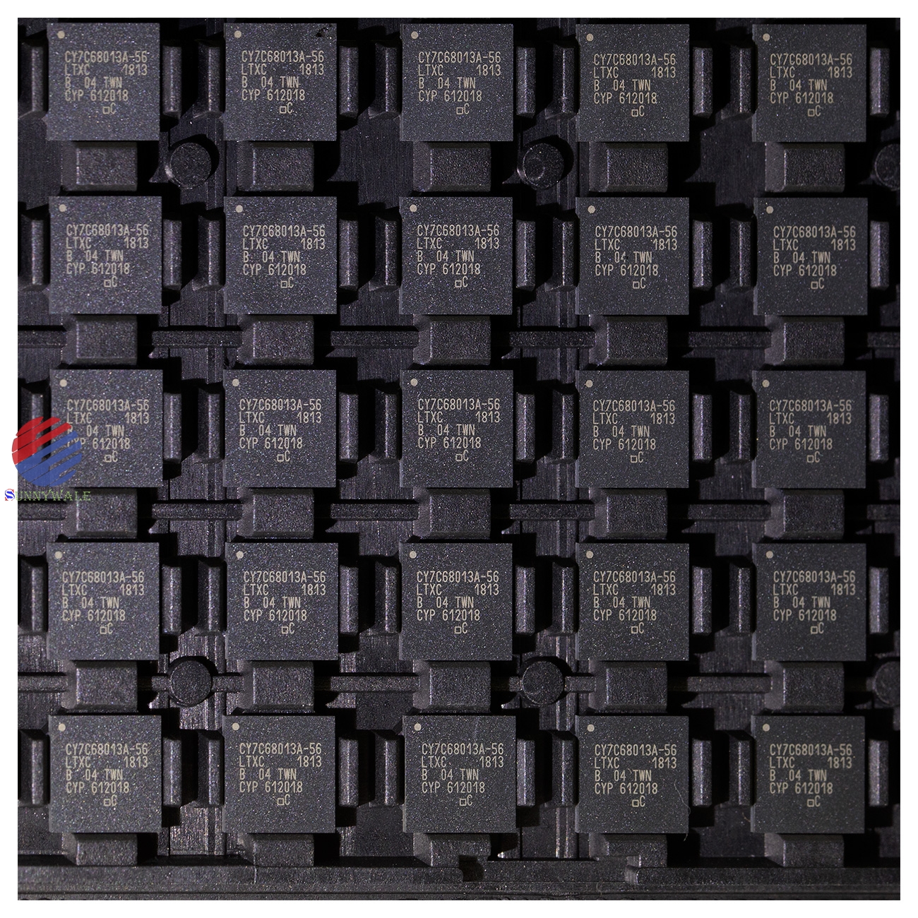
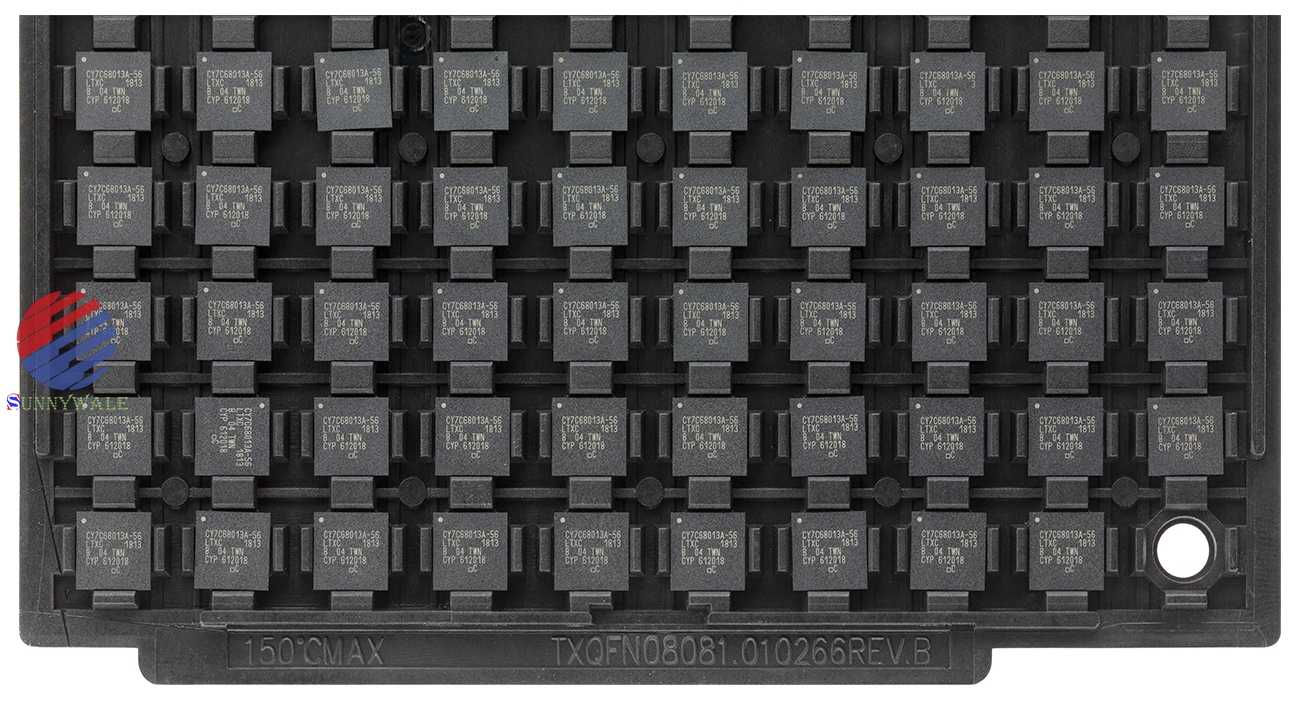
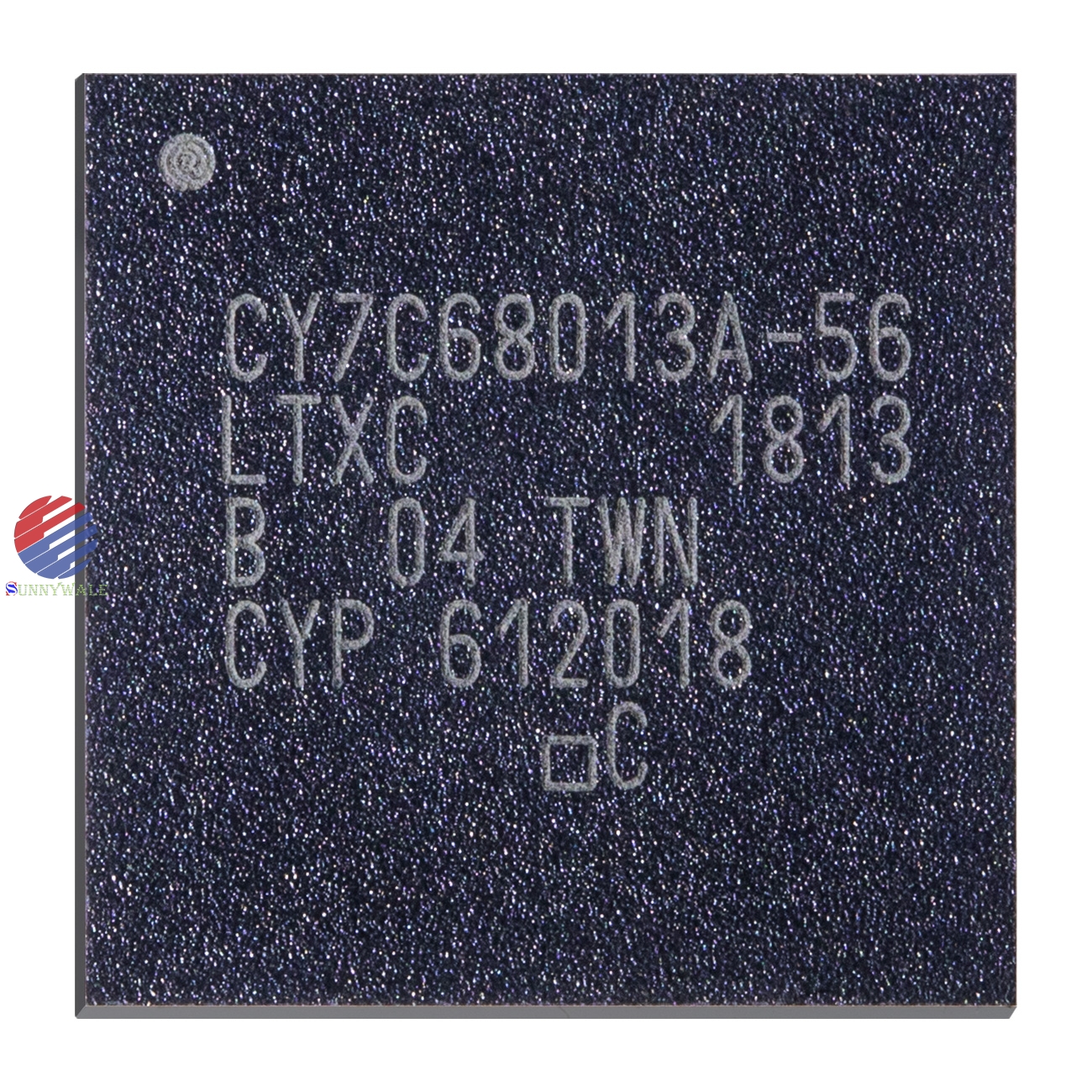
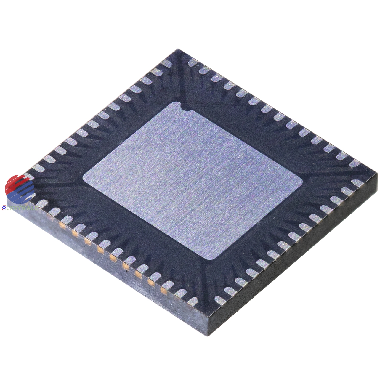
All of the above pictures are taken after matting the online showing, what you see is what you get.
Click or copy the link to free download the CY7C68013A datasheet PDF file.
Freight is free when you buy 2 pieces in China, if you have CY7C68013A inventory, you can sell to me, if you need buy CY7C68013A, you can ask me to buy.
If you want to know about similar products , or click here,or Visit The official website:
sunnywale.com,Search the keywods“**”,it can show more details.
For more details and HD images, please copy the following link to open in your browser to view our official website;or visit our official website:
Sunnywale.com , searching keyword "68013".
If you want to read the introduction in English, please Clict the
中文版